
Sign reversal of anisotropic magnetoresistance and anomalous thickness-dependent resistivity in Sr2CrWO6/SrTiO3 films
2022-10-26 09:52ChunliYao姚春丽TingnaShao邵婷娜MingruiLiu刘明睿ZitaoZhang张子涛WeiminJiang姜伟民QiangZhao赵强YujieQiao乔宇杰MeihuiChen陈美慧XingyuChen陈星宇RuifenDou窦瑞芬ChangminXiong熊昌民andJiacaiNie聂家财
Chinese Physics B 2022年10期
关键词:赵强
Chunli Yao(姚春丽) Tingna Shao(邵婷娜) Mingrui Liu(刘明睿) Zitao Zhang(张子涛)Weimin Jiang(姜伟民) Qiang Zhao(赵强) Yujie Qiao(乔宇杰) Meihui Chen(陈美慧)Xingyu Chen(陈星宇) Ruifen Dou(窦瑞芬) Changmin Xiong(熊昌民) and Jiacai Nie(聂家财)
1Department of Physics,Beijing Normal University,Beijing 100875,China
2State Key Laboratory of Luminescence and Applications,Changchun Institute of Optics,Fine Mechanics and Physics,Chinese Academy of Sciences,Changchun 130033,China
Keywords: Sr2CrWO6/SrTiO3,anisotropic magnetoresistance,sign reversal,resistivity
1. Introduction
Double perovskite is a large class of compounds discovered in the 1960s. Its chemical formula is A2BB′O6, where A is alkaline earth metal or rare earth metal ion,and B and B′are transition metal ions.[1,2]The double perovskite compound A2BB′O6takes transition-metal atoms B and B′as the center to form an oxygen octahedron ABO3and AB′O3, which alternately crystallizes in the rock salt structure along the three crystal axes. Double perovskite oxides usually have a very high Curie temperature (>400 K). High Curie temperature make double perovskite oxide a potential material for magnetoresistive devices and room temperature spintronics.[3]Febased double perovskite has been widely studied in the past few decades. High Curie temperatures in Sr2FeMoO6(TC=440 K)and Sr2FeReO6(TC=401 K)have been observed.[4,5]In 2000s, it was also discovered that the Cr-based double perovskite also has a large low-field magnetoresistance and a high Curie temperature.[6]Curie temperatures well above 600 K have been reported in the double perovskite Sr2CrReO6polycrystalline samples.[7,8]In the other Cr-based double perovskites, such as Sr2CrMoO6and Sr2CrWO6(SCWO),TCabove 450 K was observed.[9,10]
SCWO is a typical A2BB′O6-type double-perovskite oxides, where Cr3+and W5+occupy the B and B′sites, alternatively. Band-structure calculations reveal that they are ferromagnetic half-metals with highly spin-polarized transport properties at the Fermi level.[3]The correspondingTCis~460 K.[10,11]In SCWO,there is antiferromagnetic exchange coupling between Cr and W, Cr3+(3d3,s=3/2) is antiferromagnetically coupled to W5+(5d1,s=1/2), giving a net spin of 2μBper formula unit(f.u.).[1]These spin states can be explained by the fact that,when the magnetic fieldHis dominant with its large positive or negative values, all spins are aligned parallel(+3/2,+1/2)or antiparallel(-3/2,-1/2)to thezdirection,respectively.[11]Moreover,W is a 5d transition metal,4d and 5d orbits have stronger ductility compared with 3d orbits,and Coulomb repulsive potential gradually weakens in 4d and 5d. Therefore, the research process has gradually moved from 3d to 4d/5d transition metal oxides. Since the spin–orbit coupling(SOC)is proportional to the fourth power of the atomic number,the SOC intensity of 5d transition metal oxides increases to a degree comparable to the Coulomb interaction, and richer physical phenomena arise.[12]The SOC caused by the double exchange interaction is also considered to be one of the possible explanations for the origin of thin film anisotropy of magnetoresistance (MR).[13–15]Due to the complex coupling between charge state,spin state,lattice state and orbital state, anisotropic magnetoresistance(AMR)characteristics can be used to explore physics. AMR increases the possibility of using devices such as magnetic field sensors and magnetoresistive random access memory. Therefore, AMR has attracted widespread attention.[16–18]
In most cases,double-perovskite materials show negative MR, and only a few studies report the positive MR or even both the positive and negative MR.[19–21]Due to the parasitic phase,[21,22]the synthesis of single-phase, high-quality SCWO is very difficult. Therefore, only a few experimental works have been reported on SCWO.[6,10,21,22]Here,we report the successful fabrication of single-phase double-perovskite SCWO thin films by pulsed laser deposition(PLD).The conductivity, Hall effect, magnetization, MR, and AMR in the epitaxial SCWO thin films grown on SrTiO3(STO)(001)substrate is investigated.
2. Experimental details
Atomically flat single-crystal TiO2-terminated(001)STO substrates were obtained by chemical etching with NH4F buffered HF solution (pH=5.1), and subsequent were annealed at 930°C for 2 h in a pure oxygen atmosphere.[24,25]SCWO films were grown on the annealed substrates by PLD(KrF,λ=248 nm),using a polycrystalline pellet SCWO target.Before each deposition,the chamber is evacuated to a vacuum of 2×10⁻⁸Torr(1 Torr=1.33322×10²Pa).During each deposition,the substrate temperature was kept at 750°C under oxygen partial pressures of 1.2×10⁻⁶Torr,the laser repetition rate was 2 Hz and the laser energy density was 1.5 J/cm2.[21]
Atomic force microscope(AFM)was used to observe the surface morphology of thin films. The structural properties of the films were measured by using an x-ray diffractometer(Shimadzu XRD-6000). The electrical-transport and magnetization were carried out by using the standard four probe resistivity measurement and the vibrating sample magnetometer(VSM)module, respectively, in a physical property measurement system(PPMS,Quantum Design). Electrode contacts to the samples were bonded by ultrasonic wire bonding(Al wire of 25 μm diameter). The DC current for the normal state measurements was 10 μA.The temperature dependence of magnetization was also measured by using a SQUID-VSM(Quantum Design).
3. Results and discussion
It can be seen from Fig.1(a)that the surface of the SCWO films is atomically flat and shows steps from the processed STO substrate, indicating a two-dimensional (2D) nucleation and a step-flow growth mode.[26]Figure 1(b)shows the XRD pattern of a typical SCWO film deposited on a single-crystal STO(001) substrate. The film peaks appear at 22.72°and 46.40°, which are the characteristic peaks of SCWO, corresponding to (002) and (004) reflections, respectively (see Figs.1(b)and 1(c)). The correspondingc-axis lattice constant is about 7.821 ˚A, which is well consistent with the previous report(7.82 ˚A).[10]For the very thin films,the mean grain size(out-of-plane)dis well consistent with the film thickness. The full width at half maximum(FWHM)of the most intense XRD peak (004) of SCWO is routinely used to determinedusing the Scherrer formula,λd=0.9/(FWHM·cosθ), whereλis the wavelength of the filament used in the XRD machine,θis the incident angle of the same peak. The nominal thickness was usually determined by the number of laser shots and the calibrated growth rate. Four typical thin films with different thicknesses of 33.89 nm, 27.11 nm, 20.33 nm, and 13.56 nm were prepared,respectively.
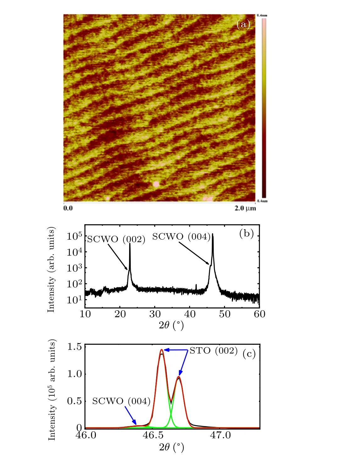
Fig. 1. (a) AFM image of a typical SCWO sample with thickness of 27.11 nm. (b) XRD pattern of the SCWO/STO (001) thin film in panel (a). (c) XRD-peak-differentiation analysis for SCWO (004) and STO(002)peaks.
The temperature dependence of the resistivity was measured by the method of four probe without an external magnetic field,which is shown in Fig.2. SCWO films,deposited under low oxygen pressure (1.2×10⁻⁶Torr), show a semiconducting behavior in the whole temperature range, which is consistent with previous reports.[6,20]We did not show the properties of SCWO films at lower temperatures than that shown in Fig. 2, because the film resistance at low temperatures is too large and exceeds the measurement range of PPMS,so some film data at lower temperatures are discarded.To our surprise,at the same temperatures,the thinner the sample, the less resistivity it has. This is intuitively contrary to the properties exhibited by most film samples.[27,28]Ohtomoet al.[29]and Kalabukhovet al.[30]have reported an extrinsic mechanism of charge doping due to the dominance of oxygen vacancies at LaAlO3/STO interfaces grown at lower oxygen pressures. In 2012, Pavlenkoet al.[31]reported that oxygen vacancies at titanate interfaces induce a complex multi-orbital reconstruction. Inspired by this, we speculate through analysis that the extrinsic mechanism of charge doping caused by oxygen vacancies is dominant at the SCWO/STO interfaces grown under low oxygen pressure (~10-6Torr). Certainly,the intrinsic oxygen vacancies in the SCWO films may also play a role. At the SCWO/STO sample,the abnormal dependence between resistivity and thickness might be related to the oxygen vacancies and the disorder in the sample. The thicker the film,the larger the carrier concentration distribution range and the higher concentration gradient there is, and therefore the higher the degree of disorder.

Fig. 2. Temperature dependence of resistivity of samples with different thicknesses. All films show semiconducting behavior in the whole temperature range. The thinner the sample,the better the conductivity.

Fig.3. Hall resistance of the SCWO films at different temperatures with the applied magnetic field up to 9 T.The slope of the curve is negative,indicating that the conductive carriers are electrons.
In order to confirm our conjecture,we performed the measurement of Hall transport(Fig.3). TheRxyshows a linear behavior up to 9 T,the negative slope of the curves indicates that the conductive carriers in SCWO are electrons. According to the formula,ns=-1/RHe,(eis the charge of an electron),the sheet carrier densitynsis obtained. The obtained sheet carrier densitynsof the films at different temperatures is shown in Fig.4(a). At the same temperatures, the sheet carrier densitynsdecreases with increase of the film thickness. It is noteworthy that in a low temperature range of 120 K–150 K,the magnitude order of sheet carrier density is the same for all films.Although this is confusing, it is speculated that this could be related to the recovery of oxygen vacancies with increase of the film thickness even under the same preparation conditions.According to the carrier mobility formula,μ=σ/nve(σis the conductivity,nvis the volume carrier density), the calculated Hall mobilityμof the films at different temperatures is shown in Fig.4(b). We can see that at the same temperatures,the thinnest sample(13.56 nm)has the largest carrier mobility.With the increase of sample thickness, the carrier mobilityμreduces significantly. From Fig.4,we can also see that for the same sample, the carrier density increases with the increase of temperature, while the carrier mobility decreases with increase of temperature. Altogether,the higher the temperature,the better the conductivity.
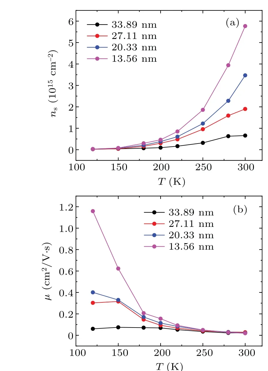
Fig. 4. (a) Temperature dependence of the sheet carrier density ns for all the SCWO films. (b)Temperature dependence of the carrier mobility μ for all the SCWO films. We can see that the thicker the sample,the smaller the carrier density and mobility.
The great difference of the thickness dependent resistivity is attributed not only to the carrier density, but also to the carrier mobility. It should be related to the specific scattering mechanism of carriers in SCWO films. The temperature dependence of resistivity of the films can be explained in terms of Mott’s variable range hopping(VRH)model.[32]According to this model,the resistivity can be expressed as
where the VRH exponentγdetermines the dimensionality of the conducting medium by the relationγ=1/(1+d). For three-,two-,and one-dimensional systems,the possible values ofγare 1/4,1/3,and 1/2 respectively.ρ(0)is the resistivity at extremely high temperature,T0is the Mott characteristic temperature, which depends on the electronic structure, and the energy distribution of the localized states.T0can be written as[33,34]

Fig. 5. (a) Resistivity data of SCWO films fitted by the VRH model. (b)Variation resistivity of SCWO films with temperature, fitted by the TA model. The solid lines represent the theoretical fitting.
wherekBis the Boltzmann constant,N(EF) is the density of states at the Fermi level andξis the localization length,i.e.,the average distance between Cr and W ions. In Fig. 5(a),lnρ(T)versus T-1/3has been plotted for all the samples,which shows a linear temperature dependence in the high temperature range.Thus,a 2D charge transport mechanism is suitable for explaining the temperature dependence of resistivity of the investigated SCWO samples. In order to estimate the value ofN(EF),we have chosen a reasonable value of the localization lengthξas,~0.39 nm,and then calculatedN(EF)from the slope of the lines in Fig.5(a)using Eqs.(1)and(2),the results are shown in Table 1.where an electron moves from one localized state to another due to an exchange of energy between the charge carrier and phonon (the localization is not a consequence of interaction with a phonon,but could occur due to a random electric field or disordered arrangement of oxygen vacancies).In Eq.(3),Wis the thermal activation energy of the electron. The electrical resistivity of is replotted as lnρ(T)versus1/Tin Fig. 5(b).Since the data do not exhibit linear behavior throughout the temperature range,we conclude that equation(3)is an inadequate description. However, this equation can provide an estimate of thermal activation energies in high temperature regions where the data can be fitted(see the Fig.5(b)). As can be seen from Figs.5(a)and 5(b),both the models describe the transport behavior of all the samples well at high temperature region.
Furthermore,the mean hopping distanceRh(T)and hopping energyEh(T) as a function of temperature are given below:[32,33]

At 300 K, calculated values ofRh(T) andEh(T) for SCWO thin films are presented in Table 1. From it,both these parameters increase with increase of the film thickness. The thermal activation energyWalso increases with increase of the film thickness. While the density of states at the Fermi levelN(EF) decreases with increase of the film thickness. Hence it gives a clear indication of disorder in the system. That is,with increase of the film thickness, the extent of disorder in the lattice increases, so that the carriers are induced in delocalized states by severe potential fluctuation. This result is well consistent with the simple estimation for the disorder:1/τ=e/m*μ, wherem*is the electron effective mass, andτis the average scattering time. As shown in Fig. 4(b), the thicker the film,the lower carrier mobilityμand therefore the high disorder.

Table 1. Physical parameters of SCWO films obtained from electrical measurements.
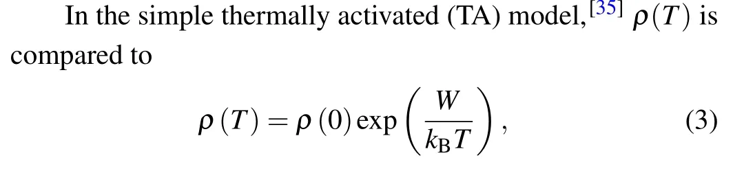
Figure 6 shows theMRat various temperatures, defined byMR=[ρ(B)-ρ(B=0)]/ρ(B=0),as a function of magnetic field(B⊥interface).[36]It is found that SCWO films all exhibit negativeMRbehavior. When the external field is 9 T,theMRcan reach 13.43%at low temperature(20 K).Negative longitudinal reluctance often occurs in magnetic materials,associated with spin-flip related scattering. As we have mentioned in our previous introduction, Cr3+and W5+are magnetic elements, and the magnetic long-range order exists in SCWO films. Therefore,SCWO exhibits negative magnetoresistance behavior.
Fig. 6. Out-of-plane negative MR as a function of the magnetic field H at various temperatures for the 13.56-nm-thick SCWO film.H is perpendicular to the current I and the interface.
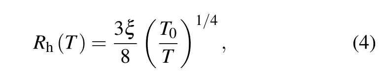
Fig. 7. Magnetization–magnetic field (M–H) curves of the typical SCWO film with thickness of 27.11 nm. All films show well-saturated M–H loops,indicating the ferromagnetic nature.
Theoretically,the antiferromagnetic coupling between Cr(S=3/2) and W (S=1/2) makes the net magnetic moment of SCWO is 2μB/f.u. along thecaxis.[11]Therefore,we measured the in-plane and out-of-plane magnetization–magnetic field (M–H) curves through PPMS at 2 K and 90 K, respectively, with a magnetic field of 0 T–9 T and the results are plotted in Fig.7.As shown in Fig.7,out-of-planeM–Hcurves show a magnetization saturation of about 1.1 (0.3)μB/f.u.at 2 K (90 K) in the field higher than 2 T, which is a little smaller than the theoretical valuation due to the anti-site defects (between Cr and W) and/or the oxygen vacancies. InplaneM–Hcurves show a magnetization saturation of about 0.7 (0.4)μB/f.u. at 2 K (90 K) in the field higher than 2 T,which is well consistent with the magnetization-temperature measurements(see Fig.8(b)).
Figure 8(a) showsAMRof the thin film as a function of the angleθfrom 0°to 360°. As is shown in the inset of Fig. 8(a),θis the angle between the out-of-plane magnetic field and the in-plane currentI.θ=0°corresponds to the configuration ofHperpendicular to the plane of the film (H⊥I),andθ=90°corresponds toHparallel to the plane of the film(H‖I)(see Fig.8(a)). Here,AMRis defined as
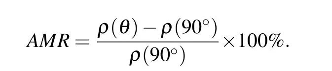

Fig.8. (a)AMR for the 27.11-nm-thick SCWO/STO(001)film,in applied field of 9 T. AMR for thin films plotted in linear coordinates with angle θ swept forward and backward (0°–360°–0°). Inset: schematic diagram of AMR measurement,where θ =0° corresponds to the direction of magnetic field H is perpendicular to the interface and the angle θ between the magnetic field direction H and z axis is varied. (b) Out-of-plane and in-plane ZFC magnetizations as a function of temperature(T)in applied field of 7 T for the SCWO/STO thin film in panel(a).
TheAMRchanges periodically with the angleθ, showing a two-fold cos2θdependence at high temperatures. Moreover, theAMRflips and changes sign as the temperature is lower than 90 K (see Fig. 8(b)). Such kind ofAMRsignal flip has never been reported in the SCWO system. This phenomenon indicates that there is a magnetic transition in the temperature between 80 K and 90 K. Therefore, we further used SQUID-VSM to measure the in-plane and out-of-plane magnetization–temperature(M–T)curves of the film at magnetic field of 7 T(maximum magnetic field in SQUID-VSM),the zero field cooling(ZFC)results are shown in the Fig.8(c).For the applied magnetic field of 7 T,Min-planeis found to be less thanMout-of-planeat temperatures belowTM~86 K.While aboveTM,theMin-planeis greater than theMout-of-plane.Therefore,we clearly observed the reversal behavior ofAMRatTM~86 K.With the decrease of temperature,the easy axis of magnetization reverses from in-plane forT >TMto out of plane forT <TM. At present,there is no clear understanding as to the reason for the change of the easy axis of magnetization. One possibility is the strain induced rotation of the magnetization easy axis. The strain originates from the difference in lattice constant between the film and the substrate.[18,37,38]SCWO/STO samples have an epitaxial strain of +0.128% in the plane of the film,since SCWO has an in-plane lattice constanta=3.91 ˚A and STO substrate has a lattice constant of 3.905 ˚A. There is another possibility that because the overall expansion ofcdecreases with increasing temperature, the reversal of the easy axis of magnetization is caused by the competition between the shape anisotropy and the inherent magneto-crystalline anisotropy.[39]
4. Conclusion
In summary, we have successfully prepared high-quality SCWO films by PLD under low oxygen pressure.All the samples show semiconducting behavior. With increase of the film thickness, a drastic resistivity increase is observed. The Hall measurements show that the thicker the film,the lower the volume carrier density. An extrinsic mechanism of charge doping due to the dominance of oxygen vacancies at SCWO/STO interfaces is proposed. The distribution and gradient of carrier concentration in SCWO films are considered to be related to this phenomenon. Resistivity behavior observed in these films is found to follow the VRH model. It is revealed that with increase of the film thickness, the extent of disorder in the lattice increases. The present study gives a clear evidence of disorder-induced localization charge carriers in these films.Magnetoresistance measurements show that there is a negative magnetoresistance in SCWO films,which is believed to be caused by the magnetic scattering of magnetic elements Cr3+and W5+. In addition, a sign reversal ofAMRin an SCWO film is observed for the first time,which is related to the direction transition of the easy axis of magnetization from out-ofplane to in-plane as the temperature increases. Our results are valuable for the application of oxide-spintronics.
Acknowledgement
Project supported by the National Natural Science Foundation of China (Grant Nos. 92065110, 11974048, and 12074334).
猜你喜欢
上海工艺美术(2021年4期)2021-04-24
妇女生活(2019年12期)2019-12-16
民间文学(2019年10期)2019-11-21
上海故事(2018年8期)2018-09-06
东方艺术·书法(2018年1期)2018-04-30
爱你(2017年31期)2017-11-24
小说月刊(2017年8期)2017-08-16
微型小说选刊(2014年27期)2014-11-17
天池小小说(2009年3期)2009-04-24
数学大世界·小学低年级辅导版(2009年3期)2009-04-14
- Chinese Physics B的其它文章
- Formation of high-density cold molecules via electromagnetic trap
- Dynamics of molecular alignment steered by a few-cycle terahertz laser pulse
- Terahertz spectroscopy and lattice vibrational analysis of pararealgar and orpiment
- Molecule opacity study on low-lying states of CS
- Finite-time Mittag–Leffler synchronization of fractional-order complex-valued memristive neural networks with time delay
- Ultrafast Coulomb explosion imaging of molecules and molecular clusters