Improved Quality Graphene Preparation Assisted by Copper Atoms and Study of Growth Mechanism
2022-12-19 09:10XUWenwenZHAOLiCHENGXiankunFANLeleZHANGYumengLIUQinzhuangLIUZhongliang
淮北师范大学学报(自然科学版) 2022年4期
XU Wenwen,ZHAO Li,CHENG Xiankun,FAN Lele,ZHANG Yumeng,LIU Qinzhuang,LIU Zhongliang
(1. School of Physics and Electronic Information,Huaibei Normal University, 235000,Huaibei,Anhui,China;2. Key Laboratory for Advanced Technology in Environmental Protection of Jiangsu Province,Yancheng Institute of Technology, 224051,Yancheng,Jiangsu,China)
Abstract:As a typical two-dimensional material,graphene has attracted broad interest. It remains a challenge to obtain the high quality graphene especially by using Molecular Beam Epitaxy(MBE). The pre-deposition of metal atom was favorable to form continual graphene structure. In this work,by means of copper atoms assistance,graphene was prepared on silicon carbide substrate by MBE technique. The influence of copper atoms amount on graphenewasinvestigated. Interestingly,an appropriate amount of copper atoms promoted the formation of graphene and the improved quality graphene was obtained. Based on experimental observation,the growth mechanism of graphene assisted by predeposition of copper atoms was studied.
Key words:graphene growth;molecular beam epitaxy;copper atoms pre-deposition
0 Introduction
As a particular two-dimensional material,graphene is a single-layer honeycomb structure[1-5],and exhibits broad promising application in solar photovoltaic devices[6],optoelectronic devices[7-8],flexible electronic devices[9-10],microelectronic devices[11-12],superconducting field effect tubes[13],and so on. High quality graphene preparation remains a hot topic and many methods such as mechanical stripping method[10],chemical vapor deposition[14-21],REDOX method[22-23],Molecular Beam Epitaxy(MBE)[24-26]have been developed to prepare single or few layers graphene. Among various methods,MBE technique demonstrates unique advantage to prepare graphene such as excellent vacuum environment that avoids impurity incorporation,controllable growth monitored by RHEED. Normally,graphene could be formed by annealing silicon carbide substrate in high temperature,while the quality of graphene needs further improvement. Considering the strong Si-C bond,the pre-deposition metal on SiC substrate was more favorable since the high active metal facilitated to bond with Si and breaks the original Si-C bond. It was reported that the pre-deposition of Hydrogen-terminated Ge was favorable to graphene transfer and tended to form continual graphene structure,owing to the weak interaction between graphene and the Ge[26]. By Ni-assistance,graphene could be constructed on silicon carbide substrate[27],while the quality of the prepared graphene needs further improvement.
Because of the uniform electronic configuration of Cu,improved quality graphene was prepared by means of copper atoms assistance,and the influence of copper atoms amount on graphene was investigated in this paper.
1 Experiments
The n-type 6H-SiC(0001)was cleaned by HF etching to remove the surface oxide,and RCA cleaning was applied to remove inorganic and organic contamination before displaced into the ultrahigh vacuum(UHV)chamber. The SiC substrate was first heated to 300 ℃to eliminate impurities such as water vapor.At the substrate temperature of 300 ℃,Cu atoms were deposited on SiC substrate and the deposition time was 5 min,10 min,20 min,30 min,40 min,respectively. All samples was annealed with substrate temperature of 1 380 ℃for 60 min.
Raman spectroscopy(type)was conducted to estimate the quality of graphene. Scanning Electron Microscopy(SEM)and Atomic Force Microscope(AFM)were carried out to observe the surface morphology.X-ray Photoemission Spectroscopy(XPS)was applied to study the electronic structure.
2 Results
Raman spectroscopy,one of the most effective tools for the analysis and characterization of graphene,was used to evaluate the quality of graphene by the location and the height of peaks[28-29]. The Raman spectra for Cu-assisted graphene were shown in Fig.1. The second order characteristic spectra of SiC substrates were observed around 1 518 cm-1and 1 723 cm-1,consistent with previous research[27,30]. Meanwhile,the existence of G and 2D peaks[27,29,31-33]confirmed the recombination of carbon sp2. It can be clearly seen from Raman diagram that the intensity of the Raman spectra corresponding to the samples obtained by directly annealing of SiC are very weak in the 2 000~3 000 cm-1range,implying poor graphene. It is obvious that the characteristic peak of graphene with copper-auxiliary becomes more prominent,indicating enhanced quality of graphene.
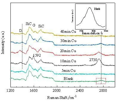
Fig.1 Raman images of the samples with different Cu pre-deposition times. The thumbnail image in the upper right corner is the result of smoothing the data in the dotted box
In order to further investigate the amount of Cu on graphene quality,Cu copper was deposited on the substrates at different time and during the same annealing process. Fig.1 showed the Raman curves of annealed silicon carbide exposed to Cu environment for different time. G peak,longitudinal optical(LO)phonon peak that was derived from mono phonons Raman scattering,was used as an important indicator to characterize graphene. It should be noted that the positions of G peaks in the all samples were around 1 600 cm-1[27,34]. The appearance of the weak D peak indicated that graphene possessed few amounts of defects[24],which was mainly derived from the corrugation,the surface dislocations and the interaction between graphene and vacancies or substrate[35]. It was interesting that the D peak for the sample with Cu pre-deposition time of 10 min exhibited the lower intensity than that of other pre-deposition time,suggesting the best quality of graphene. More or less Cu predeposition time was disadvantaged for graphene growth. By comparing the relationship between peak D and peak G,the grain size of Lawas approximately calculated(ID/IG)[28].
Table 1 shows the crystallite size(La)and ID/IGof the samples. According to the calculated La and the peak position in Raman spectra,the graphene quality was improved when time increases from 0 to 10 min.The graphene sample with Cu pre-deposition time of 10 min showed the highest G peak and lowest D peak.However,when the deposition time increased up to 40 min,the La decreased as well. The intensity ratios of D and G peak of samples are around 0. 6,which proved that there are few defects in graphene atomic crystals,and the ID/IGis far lower than previous research results[27,36]. In Table 1,the SiC substrate exposed to Cu for 10 min,the crystallite size is larger and the FWHM(full width at half maximum)is the smallest,which was confirmed the best quality of graphene at the time point.
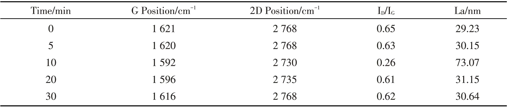
Table1 The crystallite size(La)and ID/IG of samples
The 2D peak from the two-photon effect is an important index for detecting the presence of graphene. It is worth mentioning that the 2D peak of the sample(10 min,20 min)is 2 730 cm-1. The peak shift was attributed to the strain effect caused by the interaction between silicon carbide substrate and graphene.Table 2 showed 2D and G peak offsets and ratios of samples at different time periods. Obviously,the A value of the sample supplemented with 10 min of copper is higher,which is closer to graphene stripping. For the samples(10 min),the ratio of 2D to G peak shift is 2.5:1,which was consistent with those in the literature[37]. It indicates that the graphene prepared under this condition is inclined to the exploited graphene. The simultaneous migration of G and 2D peak was due to the uniformly oriented stress between the graphene and the SiC substrate.

Table 2 The G offsets and 2D Offsets and ratio of the samples
In order to determine the composition and state of the surface atoms or ions,the samples were further characterized by XPS. Fig.2 showed the C 1 s peak of the samples. The fitting procedure showed that the C 1 s peak can be divided into three parts,with the combined energies of 284. 9 eV,284. 4 eV and 283. 4 eV which were corresponded to interface buffer layers(6 3×6 3),graphene and SiC,respectively. The peak centered at 284.9 eV was associated with carbon atoms with sp2hybridized-orbitals[36,38]. The main component of the intrinsic annealing sample was the buffer layer,whereas there were large amounts of graphene on other samples. From Fig.2(b),the results of peak division showed that the peak with combined energies of 283. 3 eV heights is low,while indicatedthe components of silicon carbide is very small. However,the peak with combined energies of 284.4 eV is very high,which indicated the content of graphene dominated. The fitting result and the actual result almost coincide.
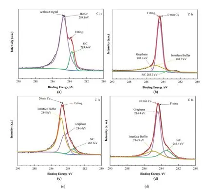
Fig.2 The XPS spectra for the samples with different Cu pre-deposition times of 0 min(a),10 min(b),20 min(c),and 30 min(d),respectively
Fig.3 showed the SEM images of the samples with different Cu pre-depositon times of 0 min(a),10 min(b),20 min(c),30 min(d),respectively. From Fig.3(a),Small particles were randomly distributed on the surface of the substrate. As shown in Fig.3(b),compared to other samples,the graphene was clearly visible,with clear contours and no obvious defects on the surface. The graphene was closely connected with each other,and there was almost no fracture. As shown in Fig.3(c),with the increase of the amount of Cu atoms,the graphene layers became thicker. The weak binding between graphene and amorphous films may be an important reason for the stable growth of high-quality graphene on the substrate. Graphene existed in the form of disperse film,and there were many holes on the surface of the sample in Fig.3(d). By comprehensive comparison,the surface pores of the sample(b)are fewer and the distribution of graphene is compact and uniform,which is the best condition for preparing high quality graphene.
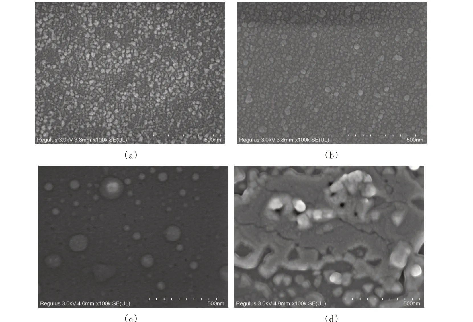
Fig.3 SEM images of the samples with different Cu pre-deposition times of 0 min(a),10 min(b),20 min(c),30 min(d),respectively
Some of the sample surface elements are shown in Fig.4. It can be seen from EDS that there was a certain amount of Si and C in the sample. Under the condition of high temperature,Cu and Si were combined to form copper silicide and left the sample surface.
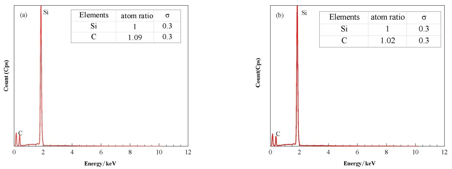
Fig.4 EDS images of the samples with Cu pre-depositiontimes of 10 min(a)and 30 min(b),respectively.The content percentages of Si and C are shown in the table on the upper right
In order to cross-check these statements,the microscopic morphology was observed by AFM. The surface morphology and 3D image of the sample exposed to Cu for 10 min were shown in Fig.5. Thin graphene was laid on the surface of the sample and the particles were evenly distributed. This is similar to the results of SEM. The maximum height of the sample is 15 nm,much lower than those of the relevant research results.
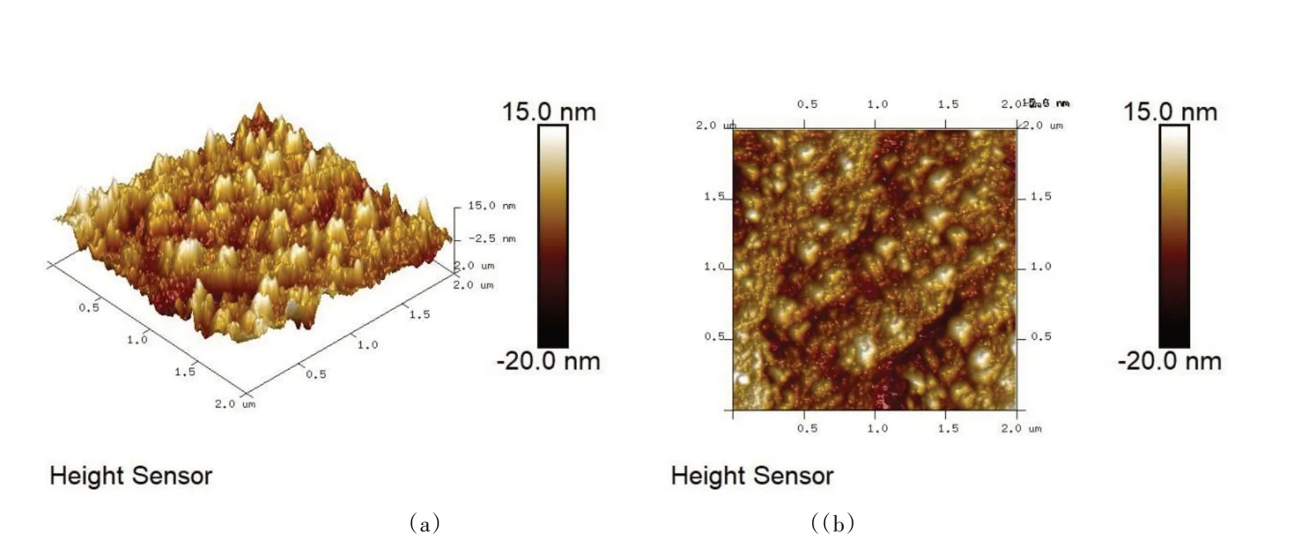
Fig.5 AFM images of the sample with Cu pre-deposition time of 10 min(a)3D profile(b)2D profile. Scale bars:2 μm
The growth principle of graphene on silicon carbide was shown in the Fig.6. Under the condition of suitable temperature,Cu atoms were slowly deposited on the surface of silicon carbide. After a period of heating,Si-C bond of silicon carbide was broken,and Cu and Si atom were combined to form copper silicide. The formation of copper silicide accelerated the rearrangement of C atoms and promoted the graphene growth under predeposition condition of the appropriate amount of Cu atoms. When the Cu content was low,a small amount of Cu atoms were difficult to bind enough Si atoms,which showed that graphene had poor crystallinity and formed discontinuous films. For the samples with predeposition condition of excess Cu atoms,some of the Cu atoms were involved in the reaction,and the remaining Cu atoms broke the surface and inhibited the formation of high-quality graphene.
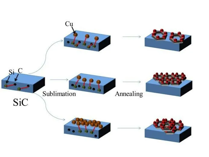
Fig.6 Schematic diagram of preparation of graphene on SiC
3 Conclusion
In summary,the improved quality graphene was prepared assisted by Cu atoms pre-deposited on silicon carbide substrate. Owing to the uniform electronic structure of copper atom,the pre-deposited copper atoms preferred to bond with silicon under high temperature,and the carbon atoms reconstructed and formed graphene. Under optimized pre-deposition condition of Cu atoms,the obtained graphene performed the best quality. Based on experimental observation and reasonable analysis,an appropriate model was provided to illustrate the growth mechanism of graphene assisted by metal predeposition. The experimental results may provide a potential approach for high quality graphene preparation in UHV condition by MBE.