
Analytical workload dependence of self-heating effect for SOI MOSFETs considering two-stage heating process
2023-10-11 07:56YiFanLi李逸帆TaoNi倪涛XiaoJingLi李晓静JuanJuanWang王娟娟LinChunGao高林春JianHuiBu卜建辉DuoLiLi李多力XiaoWuCai蔡小五LiDaXu许立达XueQinLi李雪勤RunJianWang王润坚ChuanBinZeng曾传滨BoLi李博FaZhanZhao赵发展JiaJunLuo罗家俊andZhengShengHan韩郑生
Chinese Physics B 2023年9期
关键词:李博
Yi-Fan Li(李逸帆), Tao Ni(倪涛), Xiao-Jing Li(李晓静), Juan-Juan Wang(王娟娟),Lin-Chun Gao(高林春), Jian-Hui Bu(卜建辉), Duo-Li Li(李多力), Xiao-Wu Cai(蔡小五),Li-Da Xu(许立达), Xue-Qin Li(李雪勤), Run-Jian Wang(王润坚), Chuan-Bin Zeng(曾传滨),†,Bo Li(李博), Fa-Zhan Zhao(赵发展), Jia-Jun Luo(罗家俊), and Zheng-Sheng Han(韩郑生)
1Institute of Microelectronics,Chinese Academy of Sciences,Beijing 100029,China
2University of Chinese Academy of Sciences,Beijing 100049,China
3Key Laboratory of Science and Technology on Silicon Devices,Chinese Academy of Sciences,Beijing 100029,China
Keywords: self-heating effect(SHE),silicon-on-insulator(SOI)MOSFETs,thermal transient response,workload
1.Introduction
Silicon-on-insulator (SOI) MOSFETs are widely considered in high-performance and high-reliability circuit applications.The existence of buried oxide layer greatly reduces the parasitic capacitance between source–drain and substrate, enabling the circuit to cope with high-speed operating conditions.[1,2]However, owing to the low thermal conductivity of oxides, the heat generated in the channel cannot be dissipated instantaneously, resulting in the self-heating effect(SHE).The temperature dependence of carrier mobility and saturation velocity degrades the drain current.[3–5]In practical applications, the SHE makes device output characteristic dependent on the workload.If the drain voltage variations slowly, the channel temperature will follow the changing power consumption, causing current response to oscillate and lattice temperature to increase, thereby affecting performance and complicating the evaluation of reliability behavior.This case is particularly important for circuits that carry signals with various frequency components.[6–8]For SOI devices and circuits, the effect of workload on dynamic SHE has always been a concern.
Traditional SHE characterization techniques such as gate resistance, pulsedI–Vand AC conductance extraction are difficult to realize high-speed monitor precise changes with time.[9–11]Therefore, the study of overall transient measurement of dynamic SHE of SOI MOSFETs has been lacking.Recently, an ultrafast pulsedI–Vmeasurement system has been realized,which can provide efficient electrical measurements in tens of nanoseconds.[11]Many researches have been carried out on modeling the SHE of devices.There are not only lumped models that simplify electrothermal simulations in circuit design, but also multi-stage models that consider multiple thermal diffusion paths and complex material systems.[13–16]However, there are few effective models with comprehensive considerations, and most of thermal transient modeling studies focus on cooling and rarely take into account the mechanism that is responsible for the workload-related heating processes.The importance of workload in studying the practical applications of SHE has been emphasized.[10,17–21]The dynamic SHE affected by frequency and duty cycle will further lead the performance metrics to deteriorate and the degradation effects to speed up, especially the bias temperature instability(BTI)and hot carrier degradation(HCD).However, most of these researches are based on simulation, and there is a lack of experiment-based systematic research on the relationship between workload and dynamic SHE.
In this work, we characterize the whole SHE heating and cooling process of SOI MOSFETs by ultrafast pulsedI–Vmeasurement system, and perform thermal analysis by using the technical computer-aided design (TCAD) simulation.Based on the two-stage(heating and cooling)mechanism,the thermal transient response model is extended to different transient thermal behaviors.The dependence of current oscillation amplitude and peak lattice temperature on frequency and duty cycle are studied systematically.In addition,the optimization of dynamic SHE through workload setting is discussed, and the high-frequency effect is extended by the model.
2.Experimental setup
As shown in Fig.1,the device in this work was BTS-gate nMOSFET fabricated based on 0.18-μm PDSOI process,with a gate length of 0.18 μm,gate width of 1.8 μm,Si film thickness of 400 nm,and buried oxide thickness of 300 nm.The experiments were carried out at room temperature(~293 K)by using the ultrafast pulsedI–Vmeasurement system.[9,11]During the measurement, the pulse voltage supplied by an arbitrary waveform generator is applied to the gate–drain terminal of device,experiencing rise time phase,pulse time phase,and off time phase.In terms of SHE,the on-state of the pulse acts as the heating phase of device and the off-state of the pulse functions as the cooling phase.In dynamic operation mode,we can obtain various frequencies and duty cycles by adjusting the pulse time and off time.The change of current caused by SHE can be observed in the time domain by monitoring the correlation between output current and measurement time.Here,the ultrafast pulse system can realize effective transient electrical measurement after overshoot of 20 ns.Further,using the heating chuck combined with ultrafast pulsedI–Vmeasurement can realize the corresponding relationship between current and channel temperature.[5]Thereby the thermal transient process is obtained.

Fig.1.Cross-section of PDSOI device.
3.Results and discussion
The response of SHE can bring about significant differences in electrical characteristics of SOI device.As shown in Fig.2(a), the transientId–Vdat 20 ns and the staticId–Vdat 80 μs of the device are compared through the ultrafast pulsedI–Vmeasurement system.The current at 20 ns represents the beginning of SHE,and the current at 80 μs refers to static DC with fully self-heating.In the case ofVG=VD=1.8 V, the static current is reduced by~6% compared with that in the transient state.
When operating at the circuit level, the device will be driven in the AC mode.As illustrated in Fig.2(b), the highspeed dynamic signal is applied to the device, which means that the device will experience incomplete heating process and cooling process during dynamic operation, and the SHEinduced temperature will fluctuate accordingly.With a given voltageVdinput, the lattice temperature rises.Once the voltageVdis removed, the lattice temperature will fall with time.Figure 2(c) shows the influence of dynamic self-heating on electrical characteristics.The response current decreases with the duration of the pulse increasing until it stabilizes to the same level after multiple pulses.With the cyclic accumulation of residual heat,the device reaches its corresponding peak self-heating temperatureTmax, which is the key factor affecting reliability.[18,22]There is a dynamic self-heating temperature oscillation during the on-to-off phase of the pulse, corresponding to the varying on-state response current ΔI,which reflects the stability of the electrical properties.These abovementioned effects will be discussed in depth in the following.
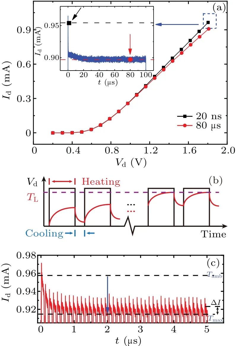
Fig.2.(a) Measured transient and static Id–Vd of SOI MOSFET,(b) schematic diagram of residual heat accumulation leading to lattice temperature rise,and(c)current response of residual heat accumulation in pulsed measurement.
3.1.Complete heating and cooling process
The SHE of device is physically determined by the heat accumulation and dissipation process inside the channel,which is characterized by ultrafast pulsedI–Vmeasurement system.The schematic diagram of the measurement principle is shown in Fig.3(a).For the heating process of the device,when the pulse voltage is turned on, the response current in the on-phase is monitored and recorded in the time domain by a high-precision oscilloscope.The decreasing process of the response current corresponds to the increase of the channel temperature.For the cooling process of the device, when the pulse voltage is turned off, two consecutive pulses with various values of cooling timetcoolthat controls the heat dissipation are used to monitor the cooling behavior.The pulse width of the first pulse determines the degree of heating.[8]Figure 3(b)shows the complete heating and cooling response curves measured.The overshoot before initial 20 ns can be clearly observed from the heating curve,and the value within overshoot should be discarded.And it can be found that the heating curve and the cooling complementary curve almost coincide.That is,the heating response and cooling response are conjugated.
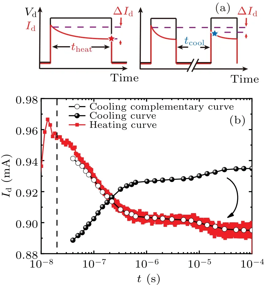
Fig.3.(a) Schematic diagram of single-pulse heating and doublepulse cooling measurement technology.(b) Measured heating current response curve,cooling current response curve,and cooling current response complementary curve.
In order to analyze the mechanism responsible for selfheating process of the device, the thermal simulation of the isolated SOI device is carried out by using TCAD.[23]The thermodynamic model is used for conducting the transport simulation to calculate the lattice temperature.The channel doping concentration is adjusted to better reflect the actual electrical characteristics of the device.Comparing theI–Vdata obtained by simulation with the experimental data shown in Fig.4(a),it can be seen that the simulation results are consistent with the experimental results.The device’s thermal path extends from the channel through the source, gate, and drain contacts to the metal interconnect above and from the channel to the substrate below.Therefore, the interconnect metal edge and the substrate bottom are used as thermodes with corresponding thermal boundary conditions.However,owing to the high thermal resistance of air free convection(2×103cm2·K/W) and the low thermal conductivity of the oxide layer surrounding the device,the upper surface and sidewalls are treated as being adiabatic relative to the heat dissipation path.In this work a surface ambient temperature of 300 K is adopted,and the surface resistance is adjusted based on Jhih-Yang Yanet al.’s research.[24]As demonstrated in Fig.4(b),the simulated channel lattice temperature is consistent with the Chuck experimental results,reaching a temperature of about 350 K.
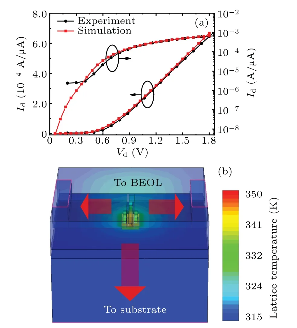
Fig.4.(a)Comparison of electrical characteristic between experimental data and simulated data, with bias condition Vd =Vg ranging from 0 V to 1.8 V.(b)Lattice temperature distribution of 3D SOI MOSFET with thermal paths.
Figure 5 shows the lattice temperature distributions of SOI device at different SHE times.When the heating starts for 1 μs, the active region with high thermal conductivity in the device is heated rapidly, which makes the heat concentrated.This is the first stage of heating process.When heated for 10 μs,the active region is sufficiently heated and acts as a heat source to diffuse heat to surrounding.The gradual conduction of heat will slowly heat the oxide layer with lower thermal conductivity,which mainly involves the second-stage heating process.After heating for 100 μs, the oxide layer is fully heated and the device reaches a stable state,with peak lattice temperatures near the drain and channel.In the conjugated cooling process, after cooling for 1 μs, the channel temperature drops rapidly,which corresponds to the heat concentrated in the active region in the first-stage heating process, being rapidly dissipated through the metal wire.After cooling for 10 μs,the heat obtained by the oxide layer with high thermal resistance around the active region through the second-stage heating process is dissipated slowly.The channel temperature is affected,thereby changing the trend of rapid decline.After cooling for 100 μs, the heat flow exits through the substrate and upper metal,and the device cools completely.Therefore,based on the material and structural properties of SOI device,the active regions and oxide layers with different thermal conductivities have a comprehensive effect on the heating process and cooling process,resulting in the two-stage SHE.
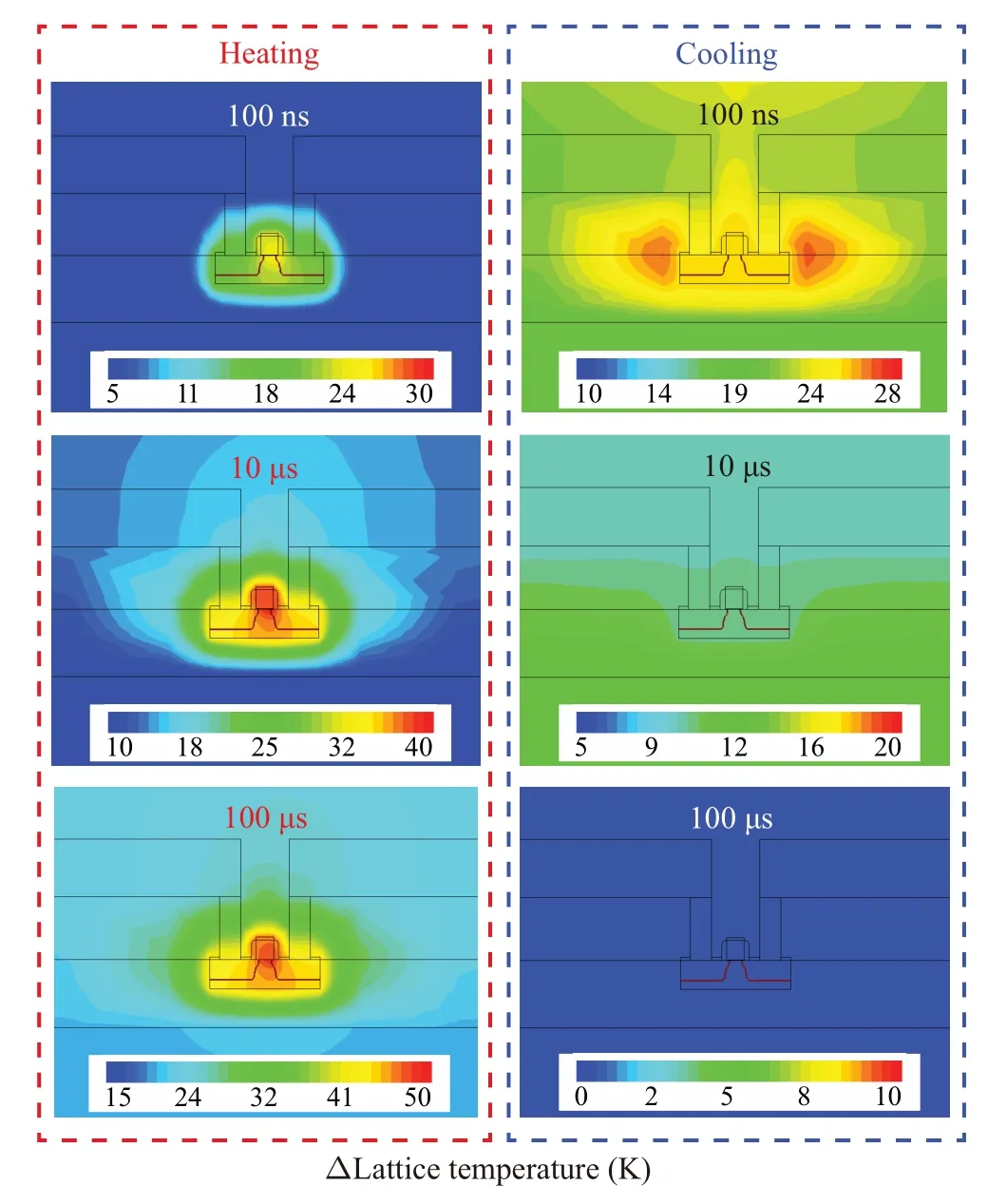
Fig.5.Simulation section maps of lattice temperature distribution at different times in complete heating and heat dissipation process.
3.2.Effective thermal transient response model
A typical thermal model for device temperature change caused by SHE consists of an equivalent circuit with thermal resistanceRthand capacitanceCthconnected in parallel.The thermal time constantτof the corresponding link in the circuit satisfiesτ=Rth×Cth.The self-heating behavior of device can be modeled by using the NID method,and the complex thermal behavior can be accommodated in the form of exponential superposition.[23,25,26]The two-stage heating process makes the device enter different stages of cooling change speed when heating times are different.Under dynamic working conditions,it is necessary to clarify the corresponding heat dissipation modes for different heating times.
Figure 6(a)shows the cooling measurement data and the cooling curves of the extracted RC model under different heating times.When the heating times are 100 μs and 10 μs, the cooling response function of the extracted model is
whereK2is the second-stage degree factor, ΔPrepresents power consumption.And when the heating times are 1 μs and 100 ns,the cooling response function is
whereK1is the first-stage degree factor.The thermal transient response is modeled as a one-stage RC model.The variations ofK1andK2with heating time are shown in Fig.6(b).The complete heating transient response curve contains two-stage heating process and is conjugated into a cooling transient response curve.Its function is
whereRth1andRth2are the first-stage and second-stage thermal resistance, respectively;τ1andτ2are the first-stage and second-stage thermal time constant, respectively.The firststage and second-stage parts of the heating transient response curve are decomposed as shown in Fig.6(b).It can be found that the changing trends ofK1andK2are respectively consistent with those of the first-stage and second-stage heating model.Combined with the above-mentioned complete heating and cooling process,the analysis is made below.
When the heating time is shorter than 1 μs, a first-order heating process is involved, and the active region of the device is heated.Corresponding to the first-stage heat dissipation mode,heat is dissipated from the active region.TheK1is determined by the degree of first-stage heating,and increases with heating time until saturation.Its expression is
When the heating time is longer than 1 μs,the active region of device is completely heated,and the second-stage heating process begins to further heat the oxide layer.Correspondingly,there is a second-stage cooling process to dissipate heat from oxide layer.TheK2is determined by the second-stage heating degree,and it becomes significant after the first-stage heating process has been completed.Its expression is
In addition,the cooling process corresponds to the heating processexactly,and the complex heating and cooling behavior of SHE can be reflected simultaneously based on the two-stage RC model.The changing trend ofK1andK2can be extended through the function,thereby expanding the cooling response.In the case of short heating time, the one-stage model can be adopted directly for simplicity.In addition, the same stage model means that the time of complete cooling is consistent.
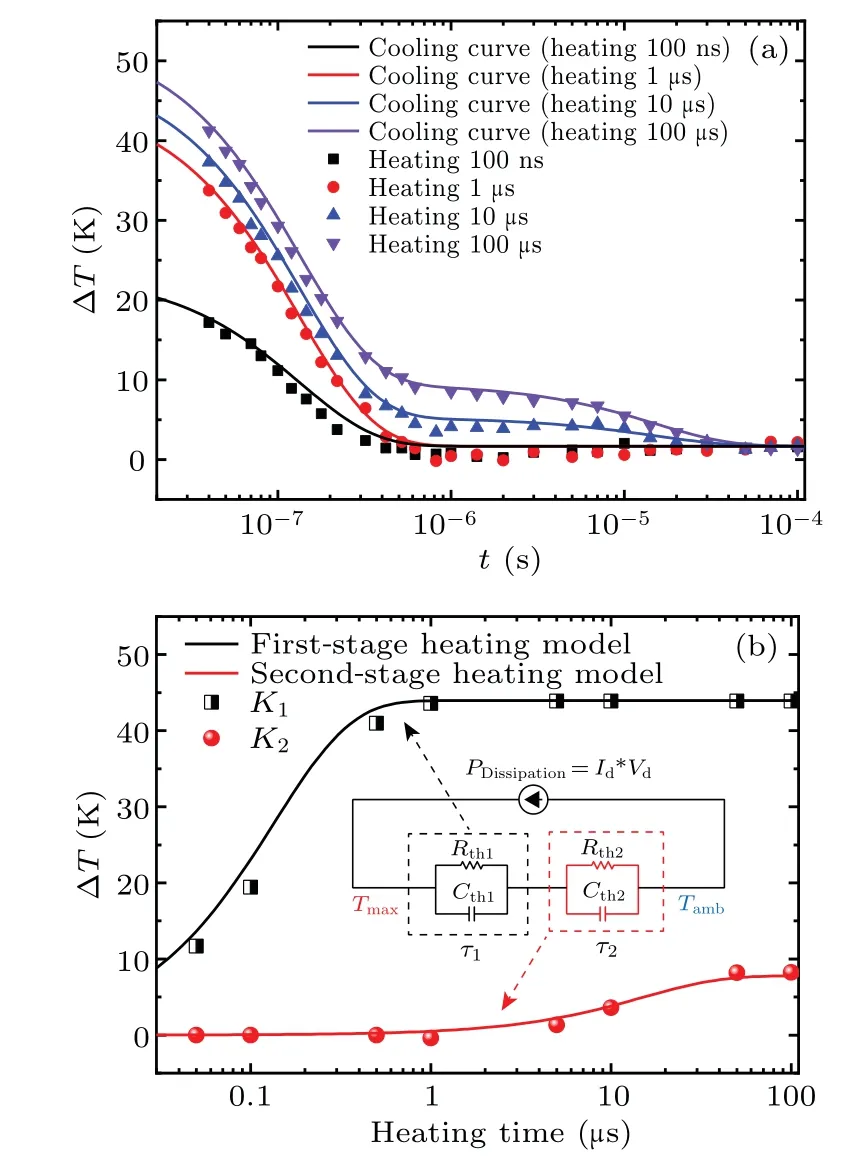
Fig.6.(a)Cooling curves of extracted RC model and measured cooling response data corresponding to different heating times.(b) Variations of K1 and K2 with corresponding heating time,and the heating response curves of each stage disassembled by two-stage heating model, with inset showing two-stage thermal equivalent RC model.
3.3.Influence of frequency on dynamic SHE
Figures 7(a)–7(c) show the response current characteristics of SOI device at different frequencies when the gate-drain voltage is set to AC mode.Figure 7(a) shows pulses at frequencies of 1 MHz, 5 MHz, and 10 MHz with a duty cycle of 50% which are applied to the gate and drain with the source grounded, corresponding to heating and cooling time of 500 ns,100 ns,and 50 ns,respectively.The comparison in the graph shows that a lower frequency results in a larger current drop.This is because the on-off state of the low-frequency signal lasts a long time,so the heat is absorbed and dissipated for a long time.In addition,owing to the short cooling time of 10 MHz and 5 MHz,the residual heat is accumulated and the response of the pulse gradually decreases.When the operating frequency reaches 1 MHz, 500 kHz, and 100 kHz, the corresponding heating and cooling times are 500 ns,1 μs,and 5 μs,respectively.As shown in Fig.7(b),the residual heat accumulation and the degree of current drop due to sufficient cooling are no longer significant.
Figure 7(c)summarizes the peak temperature and current oscillation amplitudes as a function of frequency.Combining the previous analysis, it can be concluded that when the frequency is not high enough and the on-state time is long enough, the corresponding heating time enters second-stage heating process with slow change.The frequency is changed from 50 kHz to 1 MHz, theTmaxis reduced from 342 K to 340 K, and the ΔIis only reduced by 4.7% from 6.2%.The peak temperature and current oscillation amplitudes are weakly dependent on frequency.When the frequency is high enough,the on-state time corresponds to the first-stage heating process in which the degree of heating changes rapidly.The frequency changes from 1 MHz to 10 MHz, theTmaxis reduced from 340 K to 315 K,and the ΔIis reduced from 4.7%to 0.6%.The peak temperature and current oscillation amplitude are significantly affected by frequency.
3.4.Influence of duty cycle on dynamic SHE
Figures 7(d) and 7(e) show the response current characteristics of SOI device at different duty cycles when the gate–drain voltage is set to AC mode.Figure 7(d) shows that the frequency is set to 5 MHz with a duty cycle of 25%, 50%,and 75%, respectively.The comparison in the graph shows that a higher duty cycle results in a higher degree of current droop.This is because as the duty cycle increases, the heating time increases and the cooling time decreases.Combined with the analysis above, it can be obtained that when the frequency is high enough,the change of the duty cycle to a longer on-state time corresponds to a decrease in the heating time of rapidly changing first-stage heating process.And the effect of the duty cycle change in this stage is obvious.The duty cycle decreases from 50% to 25%, the peak temperature decreases from 322 K to 306 K, and the current oscillation amplitude decreases from 1.61% to 0.77%.Under the accumulation of waste heatnd at higher temperature base,the duty cycle drops from 75%to 50%,the oscillation amplitude decreases slightly,and the peak temperature decreases significantly,from 333 K to 322 K.
However,when the operating frequency reaches 100 kHz in Fig.7(e),there is little difference in response current among different duty cycles.The oscillation amplitude variation is within 0.2%,and the peak temperature variation is within 5 K.When the frequency is not high enough, the on-state time of the different duty cycles is long enough, and the corresponding heating time triggers off a slowly changing second-stage heating process, in which the duty cycle change has a weak effect.
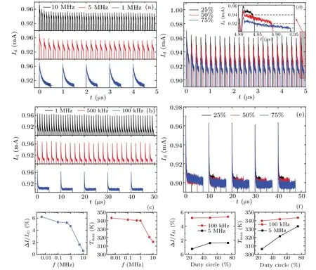
Fig.7.The Id responses of SOI MOSFET in AC mode under the Vd pulses with the same 50% duty cycle but different frequencies with frequencies being(a)1 MHz, 5 MHz, and 10 MHz,and(b)1 MHz,500 kHz,and 100 kHz respectively.(c)Summarization of the effects of frequency change on current oscillation amplitude and peak temperature,with Id1 being the current value of the first pulse at the initial 20 ns,Id referring to responses of SOI MOSFET during the AC mode under the Vd pulses with the same frequency but different duty cycles.(d)Id responses at frequency(d)5 MHz and(e)100 KHz.(f)Summaization of the effects of duty cycle changes on current oscillation amplitude and peak temperature.
3.5.Optimization of dynamic SHE
The analysis above shows that different heating times correspond to different heat dissipation modes.Therefore, the cooling time required by the device under different workload is different.Furthermore,the complete cooling time required for different heating times in the same heating process is consistent,thus providing a unified reference for the optimization of dynamic self-heating.As shown in the upper panel of Fig.8,for the second-order heating process, taking the heating time of 10 μs for example,the triple secondstage thermal time constantτ2can be used to realize complete cooling under dynamic operation,thus avoiding the accumulation of residual heat and eliminating the difference between pulses.As shown in the lower panel of Fig.8, for the first-stage heating process, we settheat=100 ns andtcool=3τ1.Not only can the accumulation of residual heat be eliminated,but also the amplitudes of current oscillations at higher frequencies are also mitigated.
The capabilities for measuring high frequencies and extreme duty cycles are limited.In such cases,the extended discussion of optimal operating strategies to suppress dynamic self-heating oscillations based on an efficient thermal model can be conducted.
Fig.8.Setting of workloads to avoid residual heat accumulation,with setting theat =10 μs and tcool =3τ1 in upper panel, and setting theat=100 ns and tcool=3τ2 in lower panel.
In terms of frequency,a fixed duty cycle of 50%is used.As shown in Fig.9(a),the amplitude of current oscillation decreases as the frequency increases.The suppression of dynamic self-heating oscillation can be divided into three intervals.For high frequencies above 10 MHz, the first-stage heating time is extremely short, resulting in a generated current oscillation amplitude of less than 1%.This interval is the best choice as dynamic self-heating oscillation is effectively suppressed.In terms of duty cycle, according to Fig.9(b),the duty cycle has little effect on the self-heating oscillation when the frequency is in the non-rapid drop interval.However, for frequencies in the rapid drop interval, the best strategy should avoid intermediate duty cycle values.Taking the case of 5 MHz for example, we should choose a small duty cycle of less than 25%to have a short first-stage heating time or a large duty cycle greater than 75%to enter a relatively stable second-stage heating process with a shorter cooling time.The dynamic self-heating oscillation is limited,and the current oscillation amplitude is less than 1%.
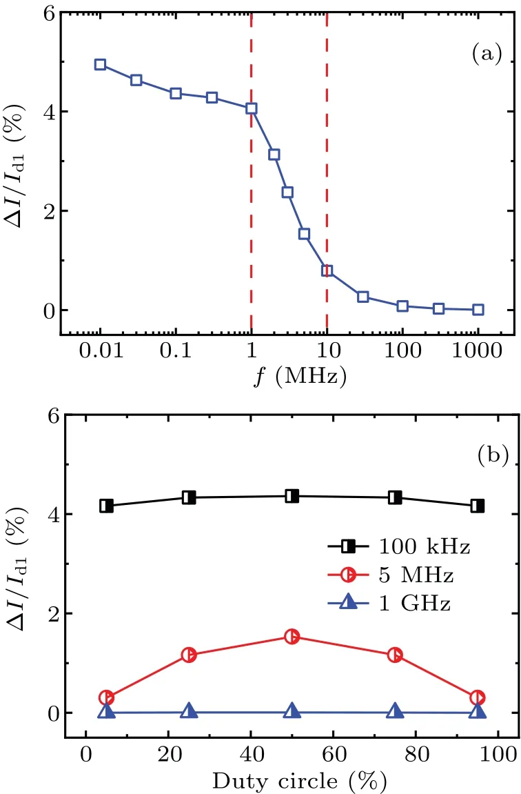
Fig.9.Current oscillation amplitude with varying(a)frequency and(b)duty cycle based on extended thermal model.
As shown in Fig.10(a),Tmaxand dynamic self-heating oscillations exhibit similar characteristics, gradually decreasing with frequency increasing.A fixed duty cycle of 50%is used.This downward trend can also be divided into three intervals.The third interval is above 10 MHz,where the correspondingTmaxdrops below 325 K,and the downward trend slows down and tends to be stable.After that, as the frequency continues to increase,the decline ofTmaxdoes not exceed 4 K.As shown in Fig.10(b),Tmaxdecreases as the duty cycle decreases.The curves converge to a single point for duty cycles of 100%and 0%.For frequencies in the first interval and second interval,Tmaxexhibits a nonlinear relationship with a decrease in duty cycle,and the downward trend is slow first and then fast.However,in the case of a high frequency of 1 GHz,theTmaxhas a linear relationship with the duty cycle,and the correspondingTmaxis only 302 K under a 5%duty cycle.From the perspective ofTmax,the optimal operating load for the device is above 10 M.Considering the linear relationship at high frequencies,setting a smaller duty cycle at this time will makeTmaxcloser to 300 K,which is more beneficial to the reliability of device.

Fig.10.Peak self-heating temperature with varying(a)frequency and(b)duty cycle based on extended thermal model.
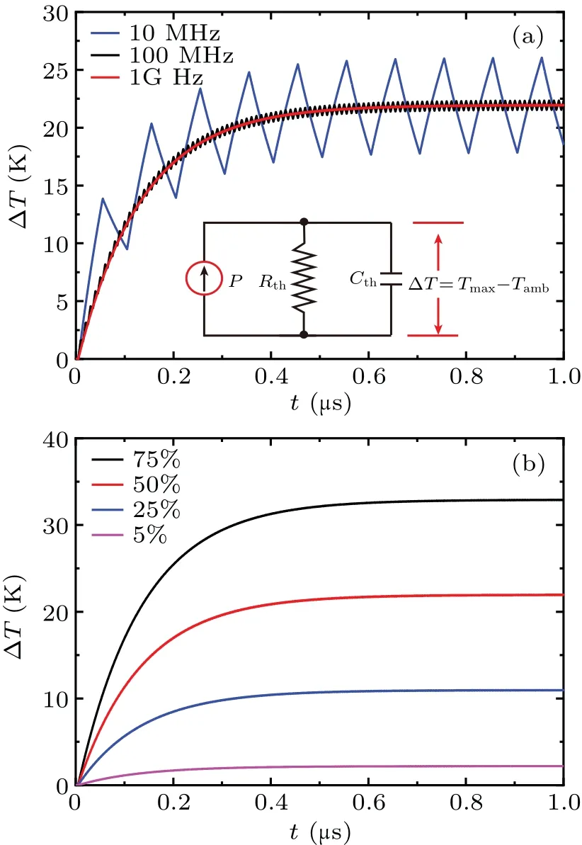
Fig.11.Model-based simulation of peak lattice temperature rise process with(a)different frequencies(the same duty cycle: 50%),with inset showing the corresponding one-stage thermal equivalent RC model,and(b)different duty cycles(the same frequency: 1 GHz).
The simulations in Fig.11 are based on a first-stage model at high frequencies.With the heating time much smaller than the first-stage thermal time constant,the dynamic self-heating oscillations of the device can be suppressed at higher frequencies.When the frequency reaches 1 GHz,the variation of heating process with time under dynamic operation is similar to a smooth curve, and the peak lattice temperature is controlled by duty cycle.When the duty cycle decreases from 50% to 5%, the ΔTdecreases by 10 times to 2.2 K,which is proportional.To sum up,the effects of workload are closely related to the two-stage mechanism of heating process.There are differences in the influence of workload at different stages on dynamic self-heating.Controlling short heating and reasonable cooling time by setting appropriate frequency and duty cycle based on two-stage mechanism can significantly alleviate SHE.And the oscillation amplitude and peak temperature can be reduced more effectively by increasing the operating frequency or reducing the duty cycle according to the onestage mode.
4.Conclusions
We comprehensively evaluated the effect of workload on dynamic SHE of SOI MOSFETs by the ultrafast pulsedI–Vmeasurement.The complete SHE heating response and cooling response of SOI MOSFETs are revealed to be conjugated,with two-stage curves shown.Based on the two-stage heating process to extend thermal transient response model, the heating time within 1 μs corresponds to one-stage simplified model,and above 1 μs corresponds to two-stage superposition model.The complete cooling times required for different heating times in the same-stage heating process are consistent.The study of dependence of workload shows that setting frequency and duty cycle control self-heating have a weak effect in the second stage, and in the first stage, the change of workload can significantly affect the peak temperature and oscillation amplitude of the response current.It is emphasized that the study of two-stage heating process can guide the unified optimization of dynamic SHE, the accumulation of residual heat can be avoided based on the thermal time constant of each stage, and the dynamic self-heating oscillation can be further suppressed at high frequencies.
猜你喜欢
Chinese Physics B(2022年11期)2022-11-21
电脑知识与技术(2022年11期)2022-05-31
Chinese Physics B(2022年5期)2022-05-16
电脑知识与技术(2022年9期)2022-05-10
Plasma Science and Technology(2022年2期)2022-03-10
Plasma Science and Technology(2021年4期)2021-04-22
Chinese Physics B(2019年10期)2019-11-06
水动力学研究与进展 B辑(2018年3期)2018-07-06
航天返回与遥感(2018年2期)2018-05-17

- Chinese Physics B的其它文章
- Dynamic responses of an energy harvesting system based on piezoelectric and electromagnetic mechanisms under colored noise
- Intervention against information diffusion in static and temporal coupling networks
- Turing pattern selection for a plant–wrack model with cross-diffusion
- Quantum correlation enhanced bound of the information exclusion principle
- Floquet dynamical quantum phase transitions in transverse XY spin chains under periodic kickings
- Generalized uncertainty principle from long-range kernel effects:The case of the Hawking black hole temperature