
Third-harmonic generation and imaging with resonant Si membrane metasurface
2023-11-08 07:55ZeZhengLeiXuLujunHuangDariaSmirnovaKhosroZangenehKamaliArmanYousefiFuDengRocioCamachoMoralesCuifengYingAndreyMiroshnichenkoDragomirNeshevandMohsenRahmani
Opto-Electronic Advances 2023年8期
Ze Zheng, Lei Xu, Lujun Huang, Daria Smirnova,Khosro Zangeneh Kamali, Arman Yousefi, Fu Deng,Rocio Camacho-Morales, Cuifeng Ying, Andrey E. Miroshnichenko,Dragomir N. Neshev and Mohsen Rahmani
Keywords: nonlinear imaging; third-harmonic generation; bound states in the continuum; membrane metasurfaces
Introduction
In recent years, the field of nonlinear nanophotonics has grown enormously and attracted tremendous attention due to a vast range of related applications, including ultrasensitive sensing1-3, optical microscopy4-6, quantum metasurfaces and entangled photon pairs generation7-12.Contributed by the development of the growth and nano-fabrication of nonlinear materials, metasurfaces have become a flexible and versatile platform for the nonlinear generations at the nanoscale13-16. By utilising the strong light-matter interaction within the subwavelength resonators, the effective nonlinearities can be significantly amplified in the nonlinear metasurfaces, as compared to their bulk counterparts17. Particularly, the optical performance of the metasurfaces can be effectively controlled via the domination of symmetry and parametric tuning18-21. Furthermore, metasurfaces made of dielectrics and semiconductors such as silicon and germanium, have been considered a promising platform for confining and manipulating light at the nanoscale based on the optically induced multipolar resonant effects22,23. Nowadays, the conception of enhanced nonlinear generations at the nanoscale has been theoretically demonstrated and experimentally achieved in various nonlinear processes, including second-harmonic generation (SHG), third-harmonic generation (THG), fourwave mixing (FWM), based on resonant dielectric metasurfaces, such as AlGaAs, GaAs, LiNbO3, and Si metasurfaces24-33. Extreme light confinement within the metasurfaces is a critical factor in achieving strong lightmatter interactions and generating nonlinear signals with higher intensity under relatively low-power input light.
Bound states in the continuum (BICs) recently emerge as a novel approach to manipulating the light-matter interactions34. The conception of BICs originates from quantum mechanics, and has now been observed and applied in metasurfaces and nonlinear generations to produce controllable light confinement within the resonators27,33,35-40. The typical dielectric metasurfaces consist of subwavelength resonators where the light is strongly confined in the vicinity of the resonators. Over the past few years, membrane metasurfaces, consisting of a single layer of nonlinear material with an array of holes, have shown unique optical properties compared to the traditional dielectric metasurfaces composed of an array of nanoparticles32,41-43. For example, membrane metasurfaces can support the resonances and maintain the nonlinear efficiency with a smaller unit-cell size compared to other platforms, offering more unit cells in the same area. This property expands the practical use of membrane metasurfaces, particularly suggesting a promising approach for improving the spatial resolution in imaging field. Besides, guided modes are widely employed in membrane metasurfaces38,44, which offer more options on manipulating the light-matter interaction, particularly in nonlinear nanophotonics.
Infrared (IR) imaging and spectroscopy based on nonlinear metasurfaces have been recognised as a potential substitute for commercial IR imaging detectors due to its superiority of being ultra-compact, containing fewer components for signal conversion45,46. Relevant works have been demonstrated based on the GaAs nanoantenna46and Si nanopillar47. What has been indicated is that improving the conversion efficiencies of nonlinear generations can facilitate the practical use of IR imaging46.
Here, we propose the employment of silicon membrane metasurfaces for augmenting THG process. Our proposed membrane metasurfaces consist of dimer holes(see Fig. 1) and can support multiple symmetry-protected BICs. By tuning the gap between the two holes, the symmetry-protected BICs can be transformed into the quasi-BICs, resulting in a strong electromagnetic field confinement within the silicon membrane via planewave illumination. Supporting multipolar resonances and concurrently maintaining small unit sizes and highmode volume for enhancing nonlinear frequency conversion is a unique advantage of membrane metasurfaces, as compared to regular particle-based metasurfaces. We reveal the formation mechanisms of the BICs by utilising the symmetry of the structure and the multipolar model. We experimentally demonstrate the conversion of near-infrared image into visible based on the THG process in membrane metasurfaces. The exploitation of membrane metasurfaces in the nonlinear generation and its closely related application, infrared imaging,can contribute to the development of the light conversion nano-device and extend its applications, particularly the infrared imaging.
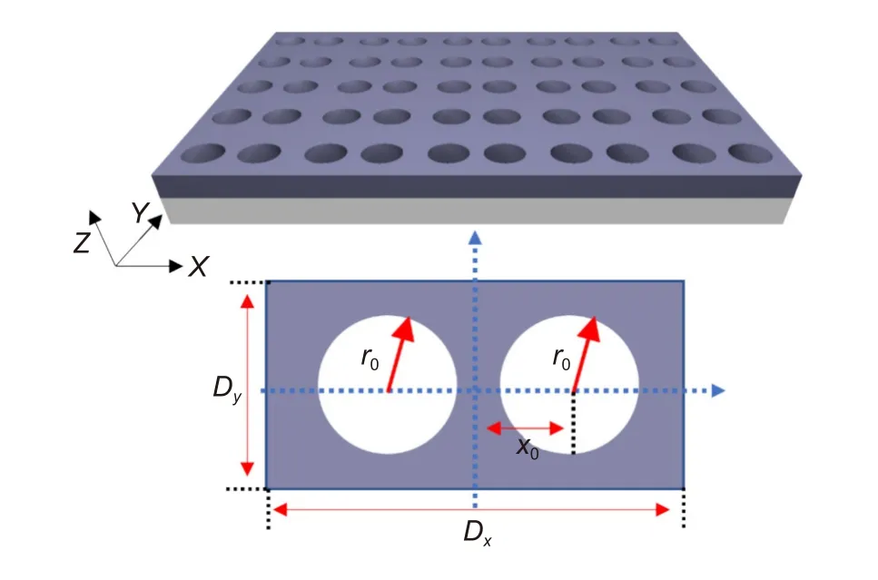
Fig. 1 | Schematic representation of the designed silicon membrane metasurface. The radius of the hole r0 is set as 100 nm.The period along x and y directions Dx and Dy are set as 600 nm and 300 nm, respectively. The offset x0 as the tunable factor is changed from 120 nm to 150 nm.
Results and discussion
Design and analysis
We consider an amorphous silicon (a-Si) membrane metasurfaces consisting of a silicon slab with dimer airy holes arranged periodically on a glass substrate, as schematically shown in Fig. 1. The radius of the hole is fixed asr0=100 nm. We define the offset parameterx0as the distance from the center of one hole to the midline of the unit (with dimer hole) along thexdirection. The period alongxandydirectionsDxandDyare set to be 600 nm and 300 nm, respectively. Thus, when the offsetx0=150 nm, the dimer-hole membrane metasurfaces will be the same as a hole membrane metasurfaces with the unit cell periodDx=Dy=300 nm. The system of the a-Si membrane metasurfaces is invariant under the 180-degree rotation around thez-axis, which is defined as the operationin this paper.
We first characterise the mode properties of such membrane metasurfaces by calculating the band structure based on the Massachusetts Institute of Technology Photonic-Bands (MPB) open sources48. Figure 2(a)shows the calculated band structure for the metasurfaces whenx0=150 nm. Here, based on modified Fabry-Perot model, we define the transverse electric modes as TE(l,m,n), wherel,m,nare the quantum numbers of the mode alongx,y, andzaxes. Specifically, the total phase accumulation is a round trip is, π(l-1), π(m-1),and π(n-1), respectively. For the considered unit cell with pitch sizes ofDx=600 nm andDy=300 nm, we observe two typical odd modes underTE(3, 1, 1) and TE(3, 1, 2) with their electric pattern M1 and M2 (see Fig. 2(b)). However, whenx0=150 nm, the pitch sizes (Dx×Dy) of unit cell changes from 600 × 300 nm to 300 × 300 nm. With the transformation of the unit cell, the two modes, TE(3, 1, 1) and TE(3, 1, 2), become even underdecoupling to the odd leaky channel to the far-field.The features of TE(3, 1, 1) and TE(3, 1, 2) indicate that they are symmetry-protected BICs with infinite Q-factor whenx0=150 nm, and can be converted into quasi-BICs with finite Q-factor when we tune the offsetx0. Meanwhile, we characterise the mode properties of silicon disk metasurfaces based on the same mode TE(3, 1, 1), which is demonstrated in Supplementary information S1.The results prove that, as compared to disk metasurfaces,membrane metasurfaces provide a powerful platform for enhancing light-matter interactions with a smaller unit cell size.
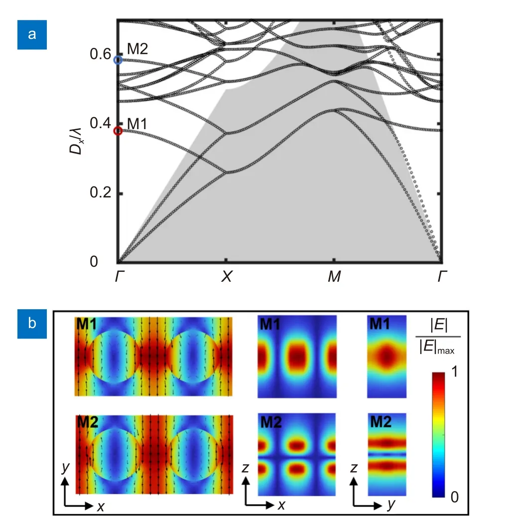
Fig. 2 | (a) Calculated bandgap structure for the metasurface with the positions of M1 (red circle) and M2 (blue circle) shown in the figure.(b) Near-field electric distributions for the mode TE(3, 1, 1) and TE(3,1, 2).
By controlling the offsetx0, one can transform such an ideal BIC into a quasi-BIC. This phenomenon has been explained from the view of symmetry. This explanation is intuitive and concise to summarise the formation of the BIC, but hardly shows the process of the energy exchange from the bound modes to the external modes.Taking Mode 1 as an example, we then investigate and characterise the modes via spherical and Cartesian multipolar analysis. This enables us to observe it from the view of multipolar transformations, manifesting itself as a Fano feature in the optical response spectrum.
We perform the spherical and Cartesian multipolar analysis49-51for three different cases:x0=120 nm, 135 nm and 150 nm, respectively. Please note that the ED, MD,EQ, MQ, EO, MO,py, and TD respectively represent the electric dipole (ED) and magnetic dipole (MD), electric quadrupole (EQ) and magnetic quadrupole (MQ), electric octupole (EO) and magnetic octupole (MO), the electric dipole moment along they-axis (py), and electric Toroidal moment (TD). As can be seen in Fig. 3, TE(3, 1,1) is dominated by ED excitation with a small contribution from the MQ and MO. The TD, MQ and MO do not contribute to the far-field radiation along thezdirection due to zero overlap with the outgoing waves. The electric dipole moment along they-axispyhere plays a role in opening a leaky channel and transforming this ideal BIC into a quasi-BIC with a finite Q-factor.

Fig. 3 | Calculated linear transmission spectra (a1-a3), spherical (b1-b3), Cartesian multipolar structures (c1-c3) and electric energy enhancement (d1-d3) inside the silicon film for the case when the offset is 120 nm (a1-d1), 135 nm (a2-d2) and 150 nm (a3-d3), respectively. In the spherical multipolar expansion, the ED, MD, EQ, MQ, EO, MO respectively represent the electric dipole (ED) and magnetic dipole (MD), electric quadrupole (EQ) and magnetic quadrupole (MQ), electric octupole (EO) and magnetic octupole (MO). In the Cartesian multipolar expansion, the py and TD represent the electric dipole moment along the y-axis (py) and electric Toroidal moment (TD).
By controlling the offsetx0, we can control the excitation and the coupling between the bright modepyand the dark mode TD, and thus control the energy exchange of the BIC with the external radiation channels,and the radiation damping rate at the resonance. When the offset increases fromx0=120 nm tox0=135 nm, the radiation damping rate and the width of the resonance decrease significantly. The radiation has decreased accordingly as the excitation of the bright modepydecreases, as illustrated in Fig. 3(c1, c2). This corresponds to a significant enhancement of the electric energy density inside the silicon film, as demonstrated in Fig. 3(d1,d2). When the offsetx0=150 nm, it corresponds to an ideal BIC where the coupling with external plane-wave under normal incidence vanishes, as revealed in Fig.3(a3-d3). From the multipolar structure, no TD excitation is observed, and the electric energy density inside the silicon film is negligible as compared to the two cases withx0=120 nm andx0=135 nm when a quasi-BIC is obtained. Figure 3 shows the process of how the leakage between the radiative channel and bound state vanishes(fromx0=120 nm tox0=150 nm).
Fabrication and characterisation
We fabricated our sample using the standard electron beam lithography (EBL). First 235 nm amorphous silicon was deposited on a glass substrate via plasma-enhanced chemical vapor deposition (PECVD). It was followed by EBL on a positive resist, called ZEP, which was used as a mask for inductively coupled plasma etching(ICP). Finally, the residual ZEP resist was removed from the surface. Figure 4(a) demonstrates the scanning electron microscopy (SEM) images of the fabricated metasurfaces sample, showing the top view and the side view(40-degree tilt). We measured and simulated the linear transmission spectrum of the metasurfaces under a white light source illumination (see Fig. 4(b, c)). Two pronounced asymmetric Fano line shapes are observed aroundλ=980nm andλ=1510nm, respectively. This indicates the excitation of the two quasi-BICs. The measured widths of the two states are around 50 nm and 20 nm, respectively.
We then measured the transmission spectra of our fabricated metasurfaces with different offsets, as shown in Fig. 5. As can be seen, the width of the resonance narrows with increasing the offset from 120 nm to 150 nm.This corresponds to the decrease in geometric asymmetry. The Fano feature in the spectrum vanishes whenx0=150 nm, corresponding to the inaccessibility of the ideal BIC supported by the metasurfaces. We also observe a slight redshift of the resonance while tuning thex0from 120 nm to 150 nm. Furthermore, we observed another Fano resonance at around the wavelength of 1000 nm. Similarly, it vanishes whenx0=150 nm. By performing the multipolar analysis, we conclude that this Fano resonance is mainly formed by the interference between the ED, EQ and MO resonances. (Multipolar structure and field distribution in Supplementary information S2)
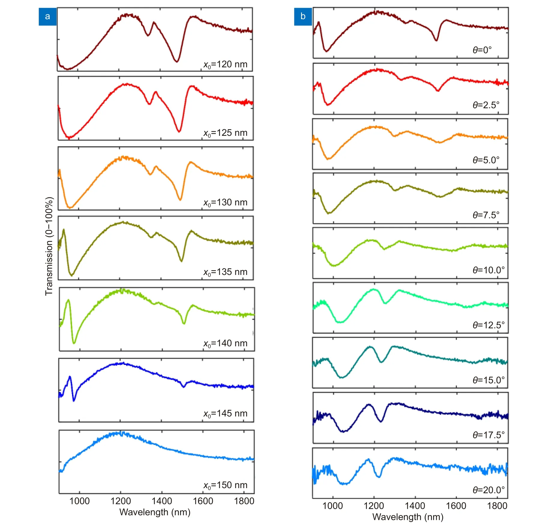
Fig. 5 | Measured linear spectra of metasurface samples with different offsets (a), and experimentally measured linear spectra of the metasurface samples with different incident angles of pump (b).
We further investigate the angular dependence of the transmission spectrum by changing the incident angleθ,of they-polarised pump light alongxzplane, as shown inθ, the redshift of the two resonances has been observed.This matches well with the calculated band structure.
TH emission was measured under the normal incidence of a pump laser with different central wavelengths.A femtosecond laser beam with 150 fs pulse width and 80 MHz repetition rate was focused to a spot size of 21μm at the sample position by an aspheric lens with a focal length of 5 cm. The pump polarisation was adjusted along theyaxis to excite the designed BIC, and the wavelength was tuned, ranging from 1400 nm to 1600 nm. The mean power on the sample plane is around 21.2 mW, leading to a maximum peak intensity value of around 1.0 GW/cm2. An objective with a numerical aperture (NA) of 0.4 was used to collect the transmitted TH emission in the forward direction, as demonstrated in Fig. 6(a). The experimentally measured TH signals from the metasurfaces with different offsets are shown in Fig. 6(b). The TH emissions are considerably enhanced at the resonance spectral position. With the offset increasing from 120 nm to 150 nm, the measured TH emission first increases to a maximum value when the offset is 135 nm, and then gradually decreases. As illustrated in Fig. 4, the width of the resonance is experimentally measured as 20 nm forx0=135 nm, this matches well with the width of our pump laser around 1500 nm, suggesting the best coupling scheme for obtaining large nonlinear emission power37. With narrower resonances obtaining higher Q-factors whenx0=140 nm andx0=145 nm, the nonlinear emission power decreases compared tox0=135 nm. It shows that a resonance with a higher Qfactor wouldn’t be beneficial under our experimental facilities. Thus, an optimised Q-factor that matches the experimentally available laser is desired for enhancing the nonlinear light-matter interaction process. When the offset is 150 nm, no significant enhancement of the TH emission is observed. This observation agrees with the fact that the ideal BIC is formed and the coupling of the BIC with external radiation has been suppressed whenx0=150 nm. The THG conversion efficiency is defined as the collected THG power divided by the incident pump power:ηTHG=PTHG/Pinput. We obtained a maximum THG conversion efficiency of around 3.6 × 10⁻⁶experimentally when the offsetx0=135 nm.
We further demonstrate the ability of THG imaging with the designed metasurfaces. Figure 7(a) shows the schematic of the THG imaging for demonstrating the ability of THG imaging by using the designed metasurfaces. A NBS 1963A resolution test target is imaged by the focal lens onto the metasurfaces. Figure 7(b1-e1) show the visible image when the metasurfaces are overlapped with the target at different positions under a white light source illumination. We then overlap the metasurfaces sample (offsetx0=135 nm) with the image of the target near the focal plane, and illuminate the target with a 1512-nm IR laser. Figure 7(b2-e2) demonstrate the images captured by a scientific CCD camera(CS165MU/M, Thorlabs). As can be seen, the pattern of the overlapping area between the image of the target and the metasurfaces (see Fig. 7(b1-e1)) can be converted to visible images clearly (as demonstrated in Fig. 7(b2-e2)).Also, this is worth noting that the dimension of our stripes (around 6 μm width at the metasurfaces plane) is sufficient to cover an array of 10 × 10 units-cells. Therefore, the boundary effect on the field enhancement driven by the non-localised quasi-BICs is insignificant. As a result, the boundary effect is not expected to have much influence on the conversion efficiency52,53. Other strategies to bypass such an issue can be employing a hybrid metal-dielectric array to design high-quality modes inspired by symmetry-protected BIC mechanism37,54. As can be seen from Fig. 7(b2-e2), we have observed a strong nonlinear emission from the designed silicon metasurfaces area, as compared to the dark background(the silicon slab area) where no sizeable nonlinear emission is detected by our camera. Moreover, among current silicon metasurfaces, membrane metasurfaces can support THG from NIR to visible with a smaller unit-cell size (300×600 nm) (indicated in Supplementary information S3)37,53,55,56. It implies a better spatial resolution for imaging.
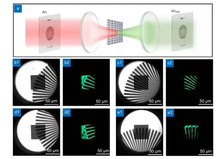
Fig. 7 | (a) The schematic of THG imaging based on Si membrane metasurfaces. The near-infrared signal passes through the target, then being converted into the visible signal via the metasurfaces, forming the target image on the CCD camera. (b1-e1) The images of the target and the metasurfaces under white light source illumination. (b2-e2) Transformed visible images of the target via membrane metasurfaces under NIR light illumination. Here the greenish colour has been used to indicate the nonlinear radiation spectrum position (504 nm). The patterns at three different positions of the target are converted to visible images clearly by the metasurfaces.
We successfully achieve the IR imaging with a clear multi-stripe pattern based on THG process. Such an approach suggests a novel platform for realising ultra-thin all-optical infrared imaging devices without the need of additional pump light. We believe that increasing the conversion efficiency of nonlinear generations based on the high-Q resonances and a large light-confined volume, such as employing light trapping assisted by slow light, increasing the spatial resolution based on small imaging units, carefully designing the optical setup to reduce the aberrations and fabricating the metasurfaces with larger areas can further improve the quality of IR imaging. In addition, compared to utilising the pump light to amplify the signal light in the SFG-based imaging, the THG-based imaging with only one input wavelength is more easily to be constructed in experiments. This simplicity may expand its application in sensing and infrared detecting.
Conclusions
In summary, we have demonstrated the potential of membrane metasurfaces for upconversion of an IR image to the visible wavelengths by the THG process based on Si material. Via tuning the offsetx0, we successfully convert the symmetry-protected BICs into quasi-BIC type resonances with infinite Q-factor. Furthermore, we reveal the formation mechanisms of those BICs from the views of symmetry and multipolar analysis. Meanwhile,after the test and characteristics of fabricated sample, we demonstrate infrared imaging as one of potential applications of enhanced THG based on Si membrane metasurfaces. The employment of membrane metasurfaces can further enhance the nonlinear generation in the aspect of offering a smaller unit size and a larger mode volume within the nonlinear material, which expands a range of applications, particularly all-optical infrared imaging at room temperature, and nonlinear spectroscopy.
Acknowledgements
Z. Zheng acknowledges the support from the Royal Society scholarship. L.Xu and M. Rahmani acknowledge support from the UK Research and Innovation Future Leaders Fellowship (MR/T040513/1). The authors acknowledge the use of NTU High Performance Computing cluster Hamilton, and the Australian National Fabrication Facility (ANFF), the ACT Node.
Author contributions
All authors commented on the manuscript.
Competing interests
The authors declare no competing financial interests.
Supplementary information
Supplementary information is available for this paper at https://doi.org/10.29026/oea.2023.220174
 Opto-Electronic Advances2023年8期
- Opto-Electronic Advances的其它文章
- A novel method for designing crosstalk-free achromatic full Stokes imaging polarimeter
- Cover
- Advancing nonlinear nanophotonics: harnessing membrane metasurfaces for third-harmonic generation and imaging
- Time-sequential color code division multiplexing holographic display with metasurface
- Direct field-to-pattern monolithic design of holographic metasurface via residual encoderdecoder convolutional neural network
- Planar peristrophic multiplexing metasurfaces