
FPGA BASED REAL-TIME VIDEO IMAGE ACQUISITION AND STORAGE SYSTEM
2012-10-08 12:10LiNa
Li Na
(School of Mathematics and Computer Science,Shaanxi University of Technology,Hanzhong,723001,P.R.China)
INTRODUCTION
Real-timevideo imageacquisition and storage moduleis an essential partin theembedded digital video system on monitoring,recording,tracking and airborne shooting[1-4]. The construction of video image acquisition and storage system based on FPGA has become a trend as the improvements of FPGA performance and integration level[5]. FPGA has on-site programmability and reconfigure ability,so the high-speed image acquisition and storage system can be realized through adopting FPGA,thereby improving the processing speed,the flexibility and the adaptability of the system[6-7].
Currently, there are many video image acquisition and storage systems implemented based on FPGA.The more popular method is to implement image acquisition or pre-processing by FPGA,and then accomplish image processing together with other CPUs[8-10].The method only implements image on-line processing in the practical application,and cannot guarantee realtime performance of storage. Furthermore,it cannot be applied when multichannel data storage is needed.Sometimes,the whole system can be realized by using one piece of FPGA[11-13],but it has the defects of small data throughput,incapable implementation of file system,and difficult acquisition of follow-up data.
Aiming at the shortcomings of existing technology, an FPGA-based video image acquisition and storage system is designed in this paper.The function modules of the whole system areimplemented in one piece of FPGA by Verilog language programming.The continuity problem of video data acquisition and storagecan be solved through double-buffering ping-pong operation,and the real-time, efficient and continuous acquisition and storage of video images can be realized through optimizing the hard disk storage rate and specific management strategies.Therefore,the system has the advantages of high integration level,good universality and strong anti-interference ability.
1 DESIGN PRINCIPLE AND HARD DISK STRUCTURE
The system mainly completes real-time acquisition and storage of analog CCD signals.And CCDanalog video decoding can becompleted with SAA7113 of PHILIPS Company.EP2C35F484C8 in CYCLONE II series of ALTERA Company is selected in FPGA on a large scale,and two pieces of IS16LV10248 are used in SRAM to complete image cache.The hard disk structure is shown in Fig.1.
FPGA is the control core of the whole system.When the system is powered on,the I2C configuration modules complete the initial configuration of SAA7113. Then the video acquisition module analyzes the video stream,extracts the valid data and generates the control signals.When receiving the frame start signal,SRAM read and write(R/W)control module stores the frame of image into SRAM in time order according to the address.After the choice of SRAM through I/O switch module, the hardware R/W control module begins to store image data into the IDE hard drive with file format. The system reserves the external bus interface,which is convenient for interface and function extension with external processors.
2 RELATED PROBLEMS AND IMPLEMENTATIONS
2.1 I2C configuration of video decoding chips

Fig.1 Structure of hard disk

Fig.2 I2Cconfiguration logic design of SAA7113
In this paper,initializing configuration is accomplished by simulating I2C protocol with FPGA which pushes the configuration parameters into the corresponding registers of SAA7113.The logic structure of the I2C configuration moduleis shownin Fig.2.The module consists of the following four parts: CLK-GEN,ROM,I2C-CMD,and I2C-CON TROL.CLK-GEN is responsible for the division of the system′s clock frequency of 100 MHz into 40 MHz,and I2C-CMD for the generation of the I2C bus control word, which includes the starting bus, the sending bus and the stopping bus.Meanwhile I2C-CMD sends the configuration parameters solidified in SAA7113 to I2C-CONTROL unit.Finally,I2C-CONTROL accomplishes the data transmission according to the reading-writing time order given by the command word.Then,on the basis of the command word, I2CCONTROL produces the R/W sequence to complete the data transmission. The whole configuration process is finished.
The following are two key points of implementing I2C protocol: Firstly,when the clock signal SCL is on the high level,the data on SDA must be steady,otherwise,it will be regarded as the start or stop signal;Secondly,when sending 8-bit address or data is finished,the bus must be released.Then,the responding signal of the bus is checked. The following operation is continued after the responding signal is obtained.Fig.3 is the working wave of I2C configuration module that is sampled by the logic analyzer named Signal Tap.It can be seen from Fig.3 that the waveform meets the timing requirements of I2C protocol.
2.2 Double-buffer ping-pong operation
As the image output is continuous,writing in hard disk takes unfixed timeduring seeking and moving magnetic heads.In order to achieve realtime video image acquisition and storage,the cache is introduced to deal with CCD image data during direct-writing in hard disk.In this paper,two ping-pong SRAM caches fairly solve the continuity of video data acquisition and storage.An image datum for PAL format is 720× 576× 2=810 KB,and the system uses two pieces of SRAMs of 1 MB,each of which can fully meet the requirements of image storage.
In Fig.4,video data streams collected by CCD are assigned to the two components of the image data buffer SRAM through the input data selection unit. Each frame image datum is a buffer cycle.In the first buffer cycle,the input data stream is cached to SRAM1,and in the second cache cycle,the video stream is cached to SRAM 2 through the input data switch unit.At the same time,the datain SRAM 1is sent to hard disk storage control module through the output data selection unit and is written in the hard disk.In the third cache cycle,the input data stream is cached to SRAM 1 through another switch of the input data selection unit,meanwhile,the second data in SRAM 2 is sent to hard disk storage control module through the output data selection unit and is written in the hard disk.Video data can be sent to hard disk for storage without any pause by cycling.

Fig.3 Logic wave of I2Cconfiguration module

Fig.4 Ping-pong buffer structure
2.3 IDE drive control strategies
Reading and writing operations of IDE hard disk must follow the ATA protocol standard,which offers two kinds of data transfer mode:PIO mode and DMA mode.The hard drive operation must use PIO mode.While to achieve high-speed data transmission,DMA mode is adopted.In this paper,PIO mode is used as control module,and Ultra DM A as w rite module to realize the high-speed and real-time video data storage.
2.3.1 PIO mode control module
PIO mode control module is mainly used to complete the configuration of the drive command register and the control register,in order to get access to the operation in the hard disk state and the initialization of DM A,and simultaneously achieve R/W operations in the hard disk with PIO mode,including such records as data read back,writing time of image data,starting position,the number of frames and so on.
Notes:(1)The hard drive after power-on does not always automatically reset successfully,so the software is needed to reset the program.Only reliable reset can make R/W operations sense.(2)Although hard disk buffer can hold more data sectors,it is necessary to inquire its state after writing in every sector in order to ensure the data reliable. Fig.5 shows the waveforms of data w riting under the control module of PIO mode collected by Signal Tap.In Fig.5,stage A is the reading status register,and ideData-In is the value;stage B is the 1F2—1F5 number register and control registers;stage C is the query register;stage D is data writing.It can be seen that the module works well.
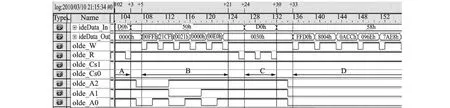
Fig.5 Logic wave of data writing in hard disk
2.3.2 Ultra DMA write module
Ultra DMA write module is used for timing design and state control during the operation to achieve thehigh-speed image data writing in disk.The system uses Ultra DMA4 with the interface rate of 66 Mb/s.Each Ultra DMA burst data transfer has four distinct operating states:Start,data transmission, suspension, and burst termination. Before the transmission of Ultra DMA,the DMA channel is initialized firstly,then the DMA request is sent to the host and the phase start state is entered,finally the data is transferred.The host sends data by switching strobe signals.
2.3.3 Optimization of hard disk transfer rate
As to a real-time video capture system,the video data are required to be stored continuously within a certain period and at a certain rate.That is, its average rate must satisfy some requirements in order not to cause memory leakage. Take Ultra DMA5 as example,the burst rateis 100 Mb/s,but when reading data of 1 MB,the average rate is only 50.18 Mb/s,mainly because thehard drive needs a longer time to locate the data position.In order to shorten time and achieve the high-speed data streams,this paper proposes two solutions to data-storing in the hard disk and drive access control,and develops some strategies to enhance the average read and write rate of the hard disk.
(1) Optimization of PIO timing control module
When transferring data block,PIO timing control module may increase transmission rate through the way of ″ahead-read″ and ″afterw rite″.The so-called ″ahead read″means that when a controller receives one read request to the ATA device data register,even if the next read request does not arrive,the controller continues to read and store data in first-in first-out(FIFO). ″After write″means that if the write operation is not yet completed,it still can accept the next w riting data from the host and store the data in FIFO.In this way,the data transmission is always continuous for the hosts and ATA devices,thereby increasing system performance.
(2)Optimization of data storage
In order to improve the data throughput speeds of IDE hard disk,it is needed to increase the rate of data transfer in hard drive and reduce the average access time.To get high-speed data streams,shortening access time becomes crucial in the study once Ultra DMA5 working mode is adopted.In the all elements,time-seeking is the main component. In order to reduce time distributing in a number of sectors of different tracks as much as possible,the disk space is directly allocated with sector as basic unit.In space coding of the sectors,a certain amount of video data are stored in chronological order in the sectors which is continuously increased on its logical address by LBA.Thus,writing to disk many times only needs to locate the position once.And it physically ensures that the least seeking time is needed in the writing operation and therefore the access time is greatly reduced.
2.4 FAT32 file management
2.4.1 FAT32 file system implementation
The hard disk can be formatted as FAT32 into four parts:Master boot record(MBR),DOS boot record(DBR),File allocation table(FAT),and the data area. Forming a recognized file system requires three steps:Firstly,to write the file directory entry to root directory area in the hard disk,which contains file-related attributes;secondly,to create the FAT table as a cluster unit in the file allocation table;finally,to write data in specified location of FAT table.Thefileis formed by state machine in this paper,and the state transition diagram is shown in Fig.6.

Fig.6 State transition of file formation
In Fig.6,S0 is the state to create file item,S1 the state to establish FAT table,and S2 the state to wait data.In the state of S3,thedata are written.The system enters into S0 after poweron or hard disk reset,establishes files directory entry in S0,and then enters S1,in which the system writes the file allocation table with end to end so that data can be stored by sectors in sequence and thus make it easy to be operated.After FAT table enters S2,the data cache stage of SRAM is completed.when one buffer is full,the system goes into S3,where data are written in the area.If there is no enough space in the disk,the system re-enters into S0 and re-records the data,otherwise,into S2 for cycle record.2.4.2 Hard disk file management strategies
As shown in Fig.7,each frame forms a file in the system design,because each frame has a fixed size,and correspondingly each file has the fixed size.Therefore,part of space can be preallocated in the data area as the storing space of directory entry,and the collected image data can be recorded on the fixed position after the catalog.
When forming a file,the size can be fixed in advance. The present file′s starting cluster number is the last file′s starting cluster number plus its file size.When filling in the FAT table,as the size of each file is fixed,the cluster numbers can be directly written in order by adding one to each number and then an ending signal is written if finished.

Fig.7 Disk file organization chart
During the recording,in order to avoid being interrupted or the overlaying of data written earlier,the system makes full use of the end of the remaining sectors of thehard disk.During the system design,a program is written in the fixed place of disk to regularly record data location and use parameters.When the system starts,it first reads the last record of the location parameter,and then writes the new data on this position.When no spaceis leftin thehard disk,the system automatically starts to record from the original position and override the older data in the hard disk,so that data is always up to date.
3 SYSTEM TEST AND RESULT ANALYSIS
When finishing design,theinner resource of FPGA is shown in Table 1.It can be seen that the wholesystem modules occupying the inner LE are about 12.66%,and the inner storage unit is about 1% and 16 multipliers.The video capture and storage system is implemented with limited resource.And there exists plenty of remaining resource, which can be used for the preprocessing algorithm or even thewhole processing algorithm.
The system is actually tested by using IBM40 GB notebook hard drive to achieve continuous acquisition and storage after power-on about 30 min.Hard disk data transfer rate is about an average of 20 Mb/s,and YUV lossless image record rate is 25 frame/s,thus achieving the full recorded real-timevideo data.Because the system directly control the hard disk,the collection storage capacity is only related to the hard disk capacity,and high-speed and large-capacity hard drives can achieve real-timevideo images of mass storage.

Table 1 Occupancy of internal resources of each module
4 CONCLUSION
In this paper,a real-time video image acquisition and storage system based on FPGA is designed in view of the disadvantages of the current system.The system uses hardwaredesign ideas so that it has the advantages of high integration, anti-interference ability, good versatility,and ease of expansion.FAT32 file system based on IDEhard disk storage has mass storage capacity and therefore it can be used for long time recording.The system has been used in a UAV ground-tracking and monitoring system to record real-time video images in UAV flight.
[1] Peng Peng,Wang Hongyuan.A control of image collection based on FPGA[J].Journal of Huazhong University of Sci&Tech,1998,26(11):14-15.(in Chinese)
[2] Mehmood K,Mrak M, Calic J,et al. Object tracking in surveillance videos using compressed domainfeatures from scalable bit-streams[J].Signal Processing:Image Communication,2009,24:814-824.
[3] Colombari A,Fusiello A,Murino V.Segmentation and tracking of multiple video objects[J].Pattern Recognition,2007,40:1307-1317.
[4] Ren Guoqiang,Wu Qinzhang,Jiang Lingtao,et al.Real-time image sampling and recording based on high-speed bus[J].Opto-Electronic Engineering,2001,28(2):53-55.(in Chinese)
[5] Guo Xiangdong. Design of video capture system based on FPGA[J].Journal of Jiujiang University,2009,155(6):15-19.(in Chinese)
[6] Monmasson E,Cirstea M N. FPGA design methodology for industrial control systems—A review [J]. IEEE Transactions on Industrial Electronics,2007,54(4):1824-1842.
[7] Zhu Changfeng, Xiao Tiejun. Design of video capture system based on FPGA[J]. Computer Engineering and Design,2008,29(17):4404-4407.(in Chinese)
[8] Singh S N,Kumar J,Panigrahi S.Hardware image compression with FPGA[J].International Journal of Recent Trends in Engineering,2009,2(8):33-35.
[9] Hirai S,Zakoji M,Tsuboi T,et al.FPGA-based realtime vision system[J]Journal of Robotics and Mechatronics,2005,17(4):Rb17-4-2344.
[10]Wang Yuzhou,Jin Shengzhen.Design of high-speed image preprocessing system based on FPGA [J].Univ Electron Sci& Tech,2005,34(1):12-15.(in Chinese)
[11]Jung Uk Cho,Seung Hun Jin,Xuan Dai Pham,et al.FPGA-based real-time visual tracking system using adaptive color histograms [C]//IEEE International Conference on Robotics and Biomimetics.Sanya,China:[s.n.],2007:172-177.
[12]Iakovidou V C. Andreadis V I. FPGA implementation of a real-time biologically inspired image enhancement algorithm [J]. J Real-Time Image Proc,2008(3):269-287.
[13]Zhang Yao,Luan Zhichao,Ouyang Yiming,et al.IDEhard disk direct-write recording based on image format[J].Opto-Electronic Engineering,2004,31(05):68-70.(in Chinese)
 Transactions of Nanjing University of Aeronautics and Astronautics2012年4期
- Transactions of Nanjing University of Aeronautics and Astronautics的其它文章
- RELIABILITY EVALUATION MODEL BASED ON DATA FUSION FOR AIRCRAFT ENGINES
- MATHEMATICAL MODEL OF 4He QUANTUM INTERFEROMETER GYROSCOPE
- EFFICIENT NUMERICAL METHOD FOR DYNAMIC ANALYSIS OF FLEXIBLE ROD HIT BY RIGID BALL
- TASK ALLOCATION BASED ON PHEROMONE
- DEVELOPMENT AND PRELIMINARY APPLICATION OF OBJECTIFYING SYSTEM FOR TCM COLOR INSPECTION
- FLIGHT CONFLICT FORECASTING BASED ON CHAOTIC TIME SERIES