
Multiple current peaks and spatial characteristics of atmospheric helium dielectric barrier discharges with repetitive unipolar narrow pulse excitation
2021-06-21 02:00XiangyuZHOU周翔宇QiaoWANG王乔DongDAI戴栋andZeenHUANG黄泽恩
Plasma Science and Technology 2021年6期
关键词:翔宇
Xiangyu ZHOU(周翔宇),Qiao WANG(王乔),Dong DAI(戴栋)and Zeen HUANG(黄泽恩)
School of Electric Power,South China University of Technology,Guangzhou 510641,People’s Republic of China
Abstract Atmospheric dielectric barrier discharges driven by repetitive unipolar narrow pulse excitation are investigated numerically by using one-dimensional fluid models.The one-dimensional simulation focuses on the effects of applied voltage amplitude,pulse repetition frequency,gap width and γ coefficient on the multiple-current-pulse(MCP)discharge.The results indicate that the MCP behavior will lead to the stratification of electron density distribution in axial direction.Traditional MCP manipulating methods,such as reducing the applied voltage amplitude,increasing the applied voltage frequency,adjusting the gap width,cannot regulate MCPs exhibiting in this work.Further analyses reveal that the increasing electric field of the cathode fall region is the basis for the emergence of MCP behavior.
Keywords:dielectric barrier discharges,narrow pulse excitation,multiple-current-pulse discharge,electric field,cathode fall region
1.Introduction
In recent decades,dielectric barrier discharges(DBDs)have been receiving great attention in both scientific and industrial fields[1–7].Typically,only one discharge current pulse is observed under each half cycle of applied voltage(Va)[8,9],and we usually regard this discharge performance as a normal operation mode.However,in some conditions,two or more current pulses will appear in each half cycle[10,11].This phenomenon,entitled the ‘multiple-current-pulse(MCP)’behavior,has been proved to weakening the discharge energy efficiency,deteriorating the regularly temporal power injection,and leading to the fluctuation of the concentration of reactive species[12–14].
For the DBD driven by conventional sinusoidal voltage,it easily evolves into filamentary discharges[15–19].However,in industrial applications,homogenous discharges are strongly demanded[20].Recently,with the breakthrough in power electronics,pulsed excitation[21]has been proved to be a promising method to improve discharge uniformity and energy efficiency[22–27].Pulsed excitation is featured on the fast rising and falling phases of Vawith millisecond to nanosecond duration.The discharge is accompanied by substantial current density and discharge intensity,achieving an efficient plasma system.To promote a large-scale industrial applications of pulsed dielectric barrier discharges(PDBDs),many groups have conducted researches on the characteristics of PDBDs[25,28–32].
The control parameters of PDBDs include applied voltage amplitude(Vam),pulse repetition frequency(f),gap width(dg),pulse rising rate(rv),etc.Previous studies have found that these parameters significantly influenced the spatiotemporal behaviors of PDBDs[33–37].Among them,the MCP phenomenon has attracted many scholars’interests.Chen et al[38]discovered that for a given rv,the number of current pulses would rise with the elevation of Vam,but each current pulse’s value would not change.In addition,Borcia et al[39]reported that when the rvwas large,there were obvious MCP phenomena.These discussions about MCP phenomenon also focused on the situation of large rising and falling phases and have drawn the conclusion that the occurrence of MCP phenomenon is related to the large pulse width.Nevertheless,there are obvious MCP phenomena when the rising and falling phases are smaller[40–43].In practical industry production,considering the discharge uniformity and energy efficiency,it is more promising to adopt pulsed power supplies with narrow pulse width.With respect to the spatial characteristics of PDBDs,Gao et al[37]studied the mode transitions of pulsed discharge and concluded that the discharge spatial
2.Fluid model
The simplified geometric configuration in figure 1 is used in our models,which has been proven to be effective in investigating the evolutions of DBDs[44–48].As can be seen,the two parallel electrodes are respectively covered by a dielectric layer with the relative permittivity of 7.5,corresponding to the value of mica glass.The gas temperature and the gas pressure are set to 300 K and 760 Torr,respectively.Considering the simplicity of the model simulation and computational burden,we use onedimensional models mainly to study the axial discharge characteristics with Vam,f and dgaltering.Note that for models shown in figure 1,electrodes are disk-shaped,and the area each is set to 0.01 m2to satisfy the prerequisite of uniform discharge.Detailed information of the operating conditions can be found in table 1.The pulse source provides repetitive direct current pulse and links to the left electrode while the right electrode is grounded.Regarding the accuracy of simulation and the requirement of the function continuity,we use a smoothed piecewise function to describe Va[49]:
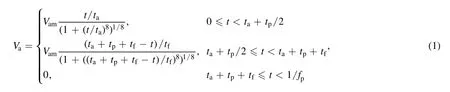

Figure 1.The geometric structure under the cylindrical coordinate system.dg and db represent the widths of the gas gap and dielectric layers,respectively.
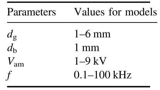
Table 1.Operating parameters set in the models.
distributions varied with voltage rising time.Admittedly,the above researches provide profound insights for PDBDs,but the mechanisms of MCP driven by narrow pulse and discharge spatial characteristics in the condition of MCP are still unclear.Accordingly,it motivates us to research the mechanisms of MCP driven by narrow pulsed power and its related spatial features for providing scientific explanation and promoting industry applications.
The outline of this paper is as follows:in section 2,the fluid models we adopted are briefly introduced;corresponding results and its relevant discussions can be found in section 3;some concluding remarks are put forward in section 4.
where Vamstands for the amplitude of Va,ta,tp,tfrepresent the pulse rise time,the plateau time and the fall time,respectively.In this paper,ta,tp,tfare set to 100 ns,400 ns,100 ns,respectively.
The simulation is developed in COMSOL Multiphysics,and the governing equations are discretized through the finite element method with a direct solver PARDISO[50].As regards the chemical reactions,we reuse one that has been validated through both 1D and 2D simulations in our previous works[13,18,19,51].To be specific,in such a set of chemical kinetics,there are 27 reactions considering the discharge process of He doped with a small amount of N2(100 ppm),and nine species are included correspondingly,that is,electron(e),.
The models used in the work is based on the fluid description with the assumption of Boltzmann electron energy distribution[52].The electron density and energy density are determined by the Boltzmann equation with drift-diffusion approximation[53].Moreover,the electron mobility is obtained by Bolsig+[54],and the Einstein’s relation[55]is adopted to calculating the electron diffusion coefficient.Meanwhile,the mobilities and diffusion coefficients for heavy species are gained from literatures[56,57].As for the transport of heavy species,the multi-component transport equation[53]is used to describe the process.Finally,Poisson’s equation[11]is coupled to make the simulation model self-consistent.Boundary conditions on the solid surfaces between dielectrics and the gas gap include the ion-induced secondary electron emission,surface charge accumulation and the metastable quenching processes.More detailed descriptions of our simulation models can be found in[13,18,19].
3.Results and discussions
3.1.Discharge phenomena
Quantities of experimental and numerical investigations[43,58–62]have shown that under an applied rectangular voltage pulse,positive and negative current pulses occur in the pulse rising and falling phases,respectively.Figure 2 illustrates the temporal profiles of Va,gap voltage,and total current when the discharge enters into steady state,in which Vam,f,and dgare set to 3 kV,10 kHz,and 2 mm,respectively.For the rising phase,when the gap voltage exceeds the breakdown voltage,the positive current pulses are produced.But,for the falling phase,considering that the polarity of current pulses is opposite to that of Va,the discharge is not directly caused by Va.During the rising phase of Va,electrons and positive ions are generated in the gas gap and accumulate continuously on the dielectric surfaces.The polarity of the spatial electric field generated by the charges is opposite to the polarity of Va.Then,when the charges accumulate to a certain extent,the gap voltage drops to zero.Therefore,when Vaenters the falling phase,with the time moving backward,Vadecreases continuously,leading to the gap voltage increasing gradually in a reverse direction.When the gap voltage exceeds the breakdown voltage,the reverse breakdown happens.
As shown in figure 2,three current pulses in the rising phase and one current pulse in the falling phase are observed,and the gap voltage has two peaks in the rising phase and one peak in the falling phase.Compared with the rising slope of Va,the gap voltage’s rising speed is slightly lower,which is consistent with the simulation results of Zhang et al[62].Regarding the relationship between the gap voltage and total current,we see that in the rising phase,a small current pulse of 3.31 A appears at t1before the first peak of the gap voltage.Then,after the gap voltage reaches the peak of 1316 V,the total current increases sharply to 16.24 A at t2,which causes the gap voltage to drop immediately.Afterwards,the gap voltage does not continue to drop,instead,it starts to increase and reaches the peak of 1195 V,which makes the total current sharply rise to 11.83 A at t3after a rapid drop,as shown in figure 2.It should be noted that in view of the fact that the first small current pulse occurs before the first gap voltage peak time,this current pulse is not caused by a new gap breakdown but the residual space charges,which not dissipate completely in the previous cycle[63].To talk about the falling phase,the discharge characteristics are simpler in contrast of the rising phase.The gap voltage reaches the peak value of −592.5 V before Vadrops to zero.The total current follows and gradually increases to the peak value of−11.60 A at t4.The peak time of total current almost coincides with the time when Vadrops to zero,which is consistent with previous reports in experiments and simulations[41,64,65].
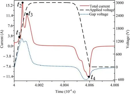
Figure 2.Waveforms of Va,gap voltage and total current when Vam is 3 kV.The current peak moments are marked in the total current curve.
By analyzing the spatial-temporal characteristics,we will obtain the discharge modes along with the evolutions,which provide a deep insight into narrow pulsed DBDs.Figure 3 presents the spatial distributions of electron density,ion density and electric field at each peak time of total current.As shown in figure 3(a),at t1,the maximum electron and ion densities are about 1017m−3.Most of space charges are concentrated near the anode side,while the space charge density at the cathode side is very small.With respect to the electric field,it almost keeps at the level of 3.14×10⁶V m−1from the anode side to 0.6 mm.It corresponds to the overlapping area of electron density and ion density,that is,the positive column region.With the decreasing distance to the cathode,the electric field increases almost linearly to about 8×10⁶V m−1.There are no obvious peaks of electron density and ion density on the cathode side.Besides,the cathode fall region is too wide and the positive column region is too small to form a mature glow discharge.In addition,although a large number of space charges distribute on the anode side,due to the existence of the positive column region,it also does not belong to Townsend discharge.The discharge is a transitional state from Townsend discharge to glow discharge.
When the second current pulse peak is formed at t2,it is obvious in figure 3(b)that the space charge density reaches about 4×10¹⁸m−3,which is close to 40 times of the space charge level in the first current pulse’s peak.Unlike the first current pulse,the peaks of electron density and ion density are located near the cathode side.There is an about 0.5 mm wide overlapping area of electron density and ion density,that is,the width of the positive column region.The cathode fall region’s width is about 0.4 mm.Based on these features,it belongs to glow discharge.Besides,it should be noted that there is a 0.2 mm wide area near the cathode where the electric field is basically kept constant at 3×10⁶V m−1,and the electron density and ion density are close to zero,which are rarely observed in alternating current(AC)DBDs[66,67].The phenomenon that the electric field remains unchanged near the cathode is also observed in[68].With the further development of the discharge,the third current peak appears at t3.In figure 3(c),it can be clearly seen that two electron density peaks and two ion density peaks are formed near the cathode side,and the horizontal area of electric field near the cathode side disappears.The maximum value of electric field increases from 3×10⁶V m−1of the second current peak to 6×10⁶V m−1at this time,and the width of cathode fall region is further narrowed from about 0.4 mm at the second current peak time to 0.2 mm at this time,which means that the discharge is further advanced in the axial space.In addition,in figures 3(b)and(c),we know that the maximum plasma density increases from about 3.75×10¹⁸m−3at t2to about 4.9×10¹⁸m−3at t3.Levko et al[69]also mentioned that the thickness of sheath becomes smaller,which means that more plasma is generated in the discharge space.Near the cathode,the ion density is no longer about zero,but 5.05×10¹⁷m−3,while the electron density is still about zero,which accords with the situation that the cathode sheath mainly has positive ions[56].It should be noted that this phenomenon of multiple electron density peaks caused by multiple current peaks has also been reported in experimental and numerical studies[58,70].However,in AC DBDs,the appearance of multiple current peaks is hard to be accompanied by multiple electron density peaks[13,71].Compared with AC DBDs,the time interval between two adjacent current pulses in DBDs driven by narrow pulse excitation is short.Therefore,it is difficult for electrons to dissipate quickly,which makes multiple current peaks accompanied by multiple electron density peaks when the DBDs are excited by narrow pulse.
As the discharge develops to the falling phase of Va,the gap voltage increases reversely mainly under the joint action of the surface charges and Va.As shown in figure 2,when the breakdown voltage is reached,the gas gap is reversely broken down,resulting in a reverse current peak at t4when Vadrops to near zero.We can see from figure 3(d)that there are three obvious electron peaks and three ion density peaks,respectively,two near the left dielectric layer(instantaneous cathode)and four near the right dielectric layer(instantaneous anode).In the vicinity of the left dielectric layer,an obvious electron density peak and an ion density peak are formed,and the cathode fall region changes from the region near the right dielectric layer in the rising phase to the region near the left dielectric layer at this time.Since the initial space charge level in the falling phase is higher than that in the rising phase,the absolute value of the maximum electric field decreases from about 6×10⁶V m−1in the third discharge of the rising phase to about 4.5×10⁶V m−1at this time.In the meantime,we notice that there are two obvious electron density peaks and two ion density peaks in the vicinity of the right dielectric layer.With the reverse of the gap voltage,under the movement of electrons and ions,the electron and ion density peaks at the right side overlap,forming a new positive column region.The peaks on the right side are mainly left by the discharges occurring in the rising phase.Since the interval between the rising phase and the falling phase is short,the space charges cannot be completely dissipated but the space charge density’s maximum value has dropped from about 7×10¹⁸m−3at t3to about 3.4×10¹⁸m−3at this time.
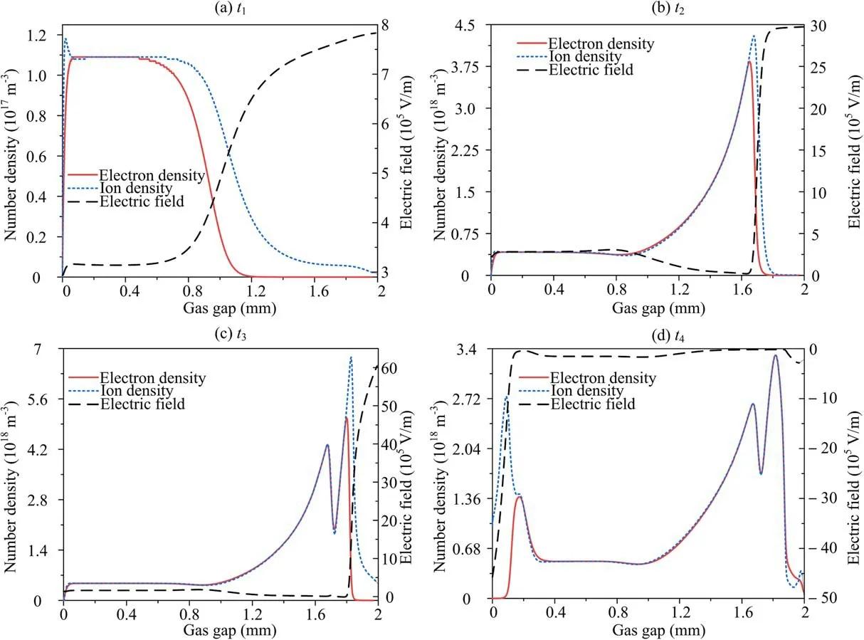
Figure 3.Spatial distributions of electron density,ion density,and electric field at current peaks.(a)–(d)Represent the distributions in t1,t2,t3,t4 marked in figure 2,respectively.
To further study the discharge characteristics,we draw the variations of electron temperature with spatial position at current peak moments,as shown in figure 4.We know that the maximum electron temperature is about 53 eV at t3,so there are no runaway electrons in this case.
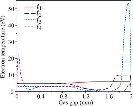
Figure 4.Spatial distributions of electron temperature at current peaks(t1,t2,t3,t4)marked in figure 2.
3.2.Can MCP be eliminated by changing Vam,f,dg,γ coefficient?
A lot of researches have been conducted on current oscillations[72–76].For MCP manipulation,common applied parameters,including Vam,f,dg,are adjusted to achieve single current pulse per half cycle when the discharge is driven by AC power supply.Many scholars have done researches on this issue[11,76,77],and they confirm that changing these applied parameters is a good way to regulate MCP phenomenon.To seek for the causes of MCP in narrow pulsed DBDs,we adopt these common control methods,which are effective in AC DBDs.To simplify the analysis,we choose the change of MCP in the positive breakdown process for discussion.
Figure 5 shows the pulse number in the positive breakdown process with Vamaltering and other parameters fixed.When Vamincreases from 1 to 9 kV,six points are selected for observation.It should be pointed out that when Vamis smaller,the points are more densely taken,and in this way we can better observe whether the low Vamcan play a regulatory role in the MCP phenomenon.We see that the number of current peaks gradually increases as Vamrises,from 1 current peak at 1 kV,3 current peaks in the range from 1.2 to 6 kV,to 5 current peaks at 9 kV.According to previous studies[12,78,79],we have known that the gap voltage peak and the current peak generally show an adjoint relationship,that is,the gap voltage peak appears first and then the current peak appears.In figure 6,the black(discrete points are represented by squares)and red(discrete points are represented by circles)curves represent the time phases of the first gap voltage peak and the second gap voltage peak,respectively.It can be clearly seen that the time phase when the first current peak appears is in front of the first gap voltage peak time,so the first current peak is not caused by a new breakdown in the gas gap when Vamranges from 1 to 9 kV.Then,the relationship between gap voltage peak and current peak can be roughly divided into two stages.The first stage is that one gap voltage peak causes the formation of several subsequent current peaks when Vamis 1.2 and 1.5 kV.As Vamfurther rises to 3 kV and above,it enters the second stage,that is,two gas gap voltage peaks cause the formation of subsequent current peaks.Therefore,after gas gap breakdown,even if there is no new gap voltage peak,the new current peaks will still be formed.Considering that there is no gap breakdown when Vamis 1 kV,although the pulse number is 1 at this time,it is not an effective manipulation of MCP phenomenon.
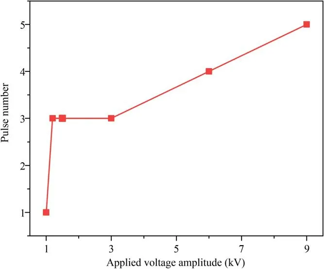
Figure 5.Pulse number as a function of Vam.
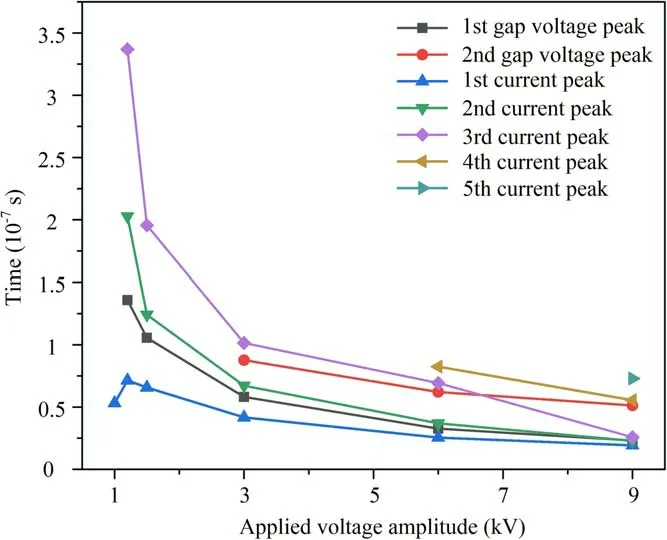
Figure 6.Time phases as a function of Vam for various orders of current peaks.
In addition to Vam,f and dgare the other important factors for manipulating MCP phenomenon.Figures 7(a)and(b)show the pulse number as a function of f and dgin the positive breakdown process,respectively.The range of f increases from 0.1 kHz to 100 kHz,and is analyzed at 0.1,1,5,10,20,40,60,80,100 kHz respectively.When f changes,the number of current peaks in the positive breakdown process is 4 at 0.1 kHz,and at the rest frequency ranges is all 3,as shown in figure 7(a).For dg,it increases from 1 mm to 6 mm with other parameters fixed.Taking a point every 1 mm,we see in figure 7(b)that the number of pulses changes from 3(1−4 mm)to 2(5−6 mm)in the process of gradually increasing dg.Considering the similarity of the process of changing Vam,the time phases as a function of f and dgfor various orders of current peaks are not present here.But some important conclusions can also be drawn from those cases.First,the current peak before the gap voltage peak is formed by the directional movement of residual charges under the gap voltage;second,whether there will be multiple current peaks after the first gap voltage peak has little to do with whether there will be new gap voltage peaks later.
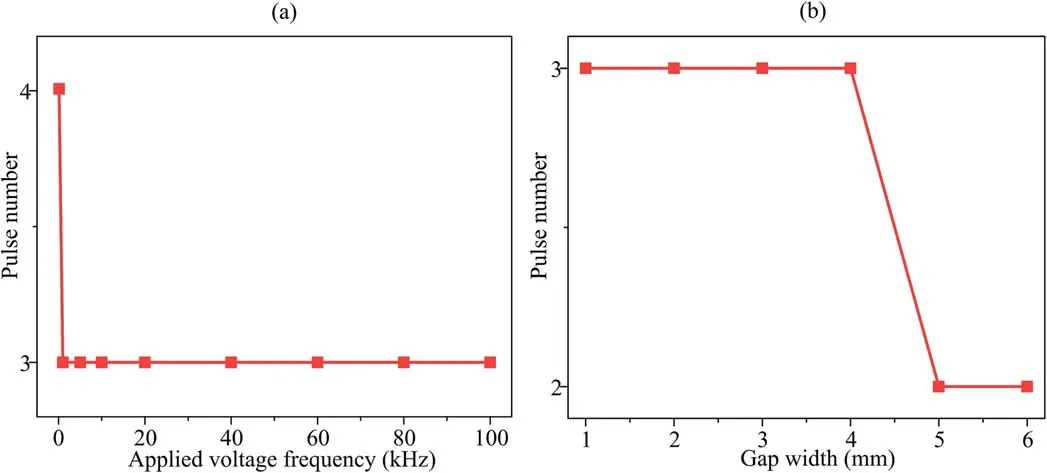
Figure 7.Pulse number as a function of f(a)and dg(b).
Therefore,traditional control methods,such as changing Vam,f and dg,are not effective in narrow pulsed DBDs.
Except for adjusting Vam,f and dgin DBDs,Y B Golubovskii et al[8,74,80]believe that the MCP phenomenon is mainly caused by the time needed for positive ions to move from anode to cathode.That is to say,the γ process on the cathode surface is a very important factor for the MCP phenomenon.To further understand the phenomena of MCPs in narrow pulsed DBDs,we explore the change of MCP phenomenon when γ coefficient is set to zero.As shown in figure 8,when γ coefficient is set to zero,it means that the positive ions cannot generate electrons by impacting the cathode,and this way of generating MCP phenomenon is eliminated.But it does not meet expectations,as can be seen,in the positive breakdown stage,there are three current peaks and two gap voltage peaks,and the MCP phenomenon does not disappear although γ coefficient is set to zero.Still and all,it should be noted that,by comparing the total current waveforms in figures 2 and 8,the value of the first current peak changes little,the value of the second current peak decreases from 16.24 to 9.04 A,and the value of the third current peak decreases from 11.83 to 5.16 A.It is attributed to the fact that the emission process on the cathode surface makes more electrons generated in the breakdown process,which will help to increase the total current.Therefore,setting γ coefficient to zero can only reduce the value of current peak,but can not make the MCP phenomenon disappear.It is consistent with the previous report[58].
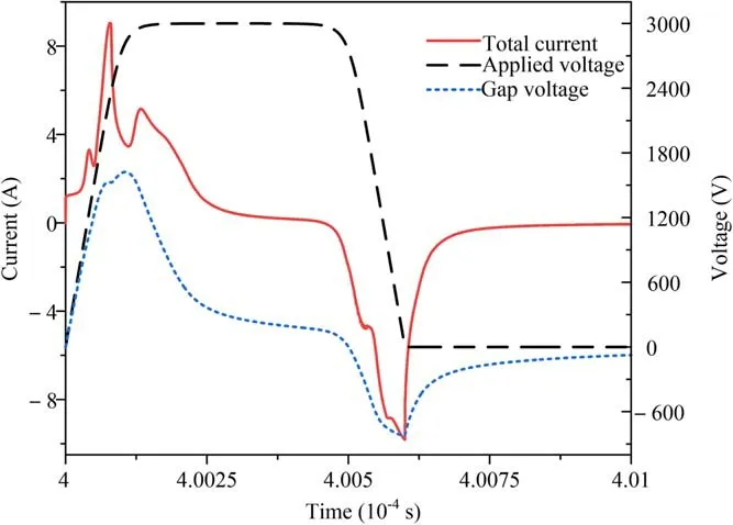
Figure 8.Waveforms of Va,gap voltage as well as total current when γ coefficient is set to zero.
3.3.Mechanisms
In order to better understand the reason why the MCP phenomenon occurs,we take Vam=1.2 kV as an example to explain the discharge characteristics.
In figure 9,there are three current peaks and one gap voltage peak in the positive breakdown stage.The first current peak is caused by the directional movement of residual space charges under the action of gap voltage,as mentioned earlier.After the gap voltage increases to the breakdown voltage,the second current peak is formed.Then,the gap voltage keeps falling as shown by the blue dotted line in figure 9,but the new current peak is formed after the second current peak.This is different from the MCP phenomenon observed in AC DBDs,where the MCP phenomenon is often accompanied by the gap electric field oscillation[11,72].We know that the formation of current peak is closely related to the spatial charge densities and electric field.To figure out why a new current peak appears when the gap voltage drops,we select the typical times marked by black dots in figure 9 to observe the spatial distributions of charge densities and electric field in figure 10.
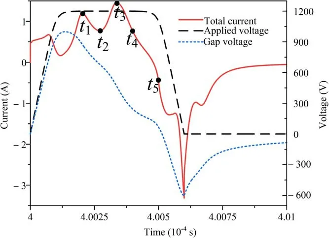
Figure 9.Waveforms of Va,gap voltage as well as total current when Vam is 1.2 kV.Some typical moments are marked in the total current curve.
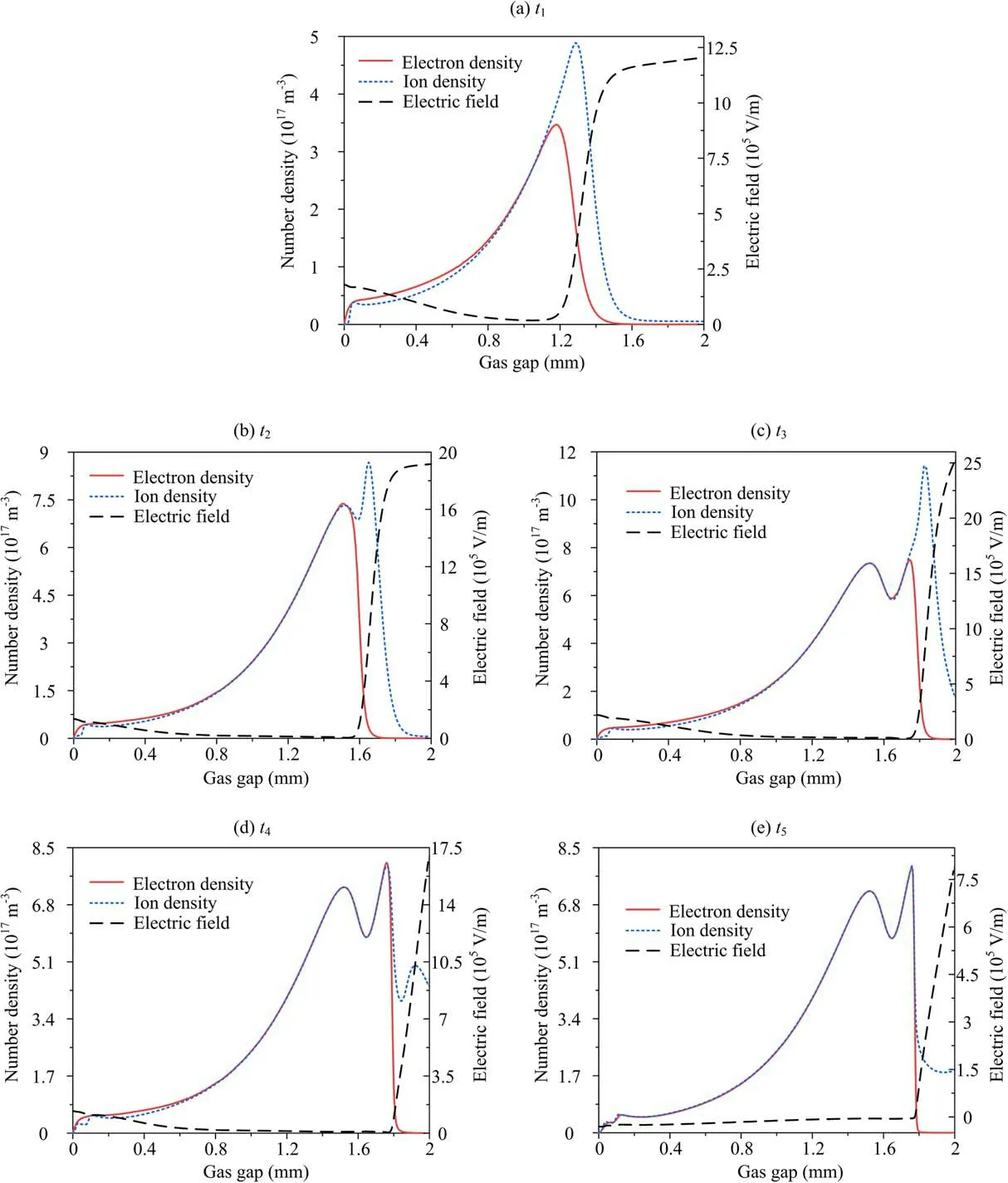
Figure 10.Spatial distributions of electron density,ion density,and electric field at typical moments marked in figure 9.
At the second current peak time t1,as can be seen from the figure 10(a),there are one electron density peak and one ion density peak in the gas gap,and the width of the cathode fall region is about 0.8 mm.At this time,the maximum electric field in the cathode fall region is about 1.2×10⁶V m−1.As the discharge time moves to the trough time t2,it can be seen from the figure 10(b)that the electron density peak remains unchanged at this time,while a new ion density peak forms on the right side of the original ion density peak.The cathode fall region’s width is also narrowed from about 0.8 mm of the second current peak to 0.4 mm.The space charge level increases from about 5×10¹⁷m−3to about 9×10¹⁷m−3.At this time,the maximum electric field of the cathode fall region is about 1.9×10⁶V m−1.
When the third current peak is formed at t3,a new electron density peak is formed on the right side of the original electron density peak in the figure 10(c).The cathode fall region’s width is further narrowed to about 0.3 mm,and the space charge level is also increased to about 1018m−3.At this time,the maximum electric field in the cathode fall region is about 2.5×10⁶V m−1.When the discharge time moves further backward to t4,as can be seen from the figure 10(d),the electron density peaks remain unchanged at two,while the ion density peaks become three.The cathode fall region’s width does not continue to narrow,and the space charge level also drops to about 8×10¹⁷m−3.At this time,the maximum electric field in the cathode fall region is 1.7×10⁶V m−1.When the discharge time goes further backward to t5,as can be seen from the figure 10(e),the electron density peaks keep two unchanged.The rightmost ion density peaks disappear,leaving only two ion density peaks,and the width of the cathode fall region has little change.At this time,the maximum electric field in the cathode fall region is about 8×10⁵V m−1.
From the above descriptions,we know that after the second current peak,a new ion density peak is formed first,then the cathode fall region’s width is continuously narrowed,the maximum electric field is keeping increased,and finally a new electron density peak is formed.After that,the maximum electric field of the cathode fall region decreases.Although the third ion density peak is formed later,the electric field does not continue to increase,so no new electron density peak and no new current pulse are formed.It should be pointed out that for the formation of the new ion density peak in the process of current pulse decline,it is mainly attributed to the fact that the ions are constantly moving towards the cathode,and the discharge at the original peak position is weakened at this time.
As can be seen,the formation of the subsequent current pulse is mainly marked by the formation of the new electron density peak,which lags behind the formation of the new ion density peak.To form a new electron density peak,the maximum electric field of the cathode fall region needs to be continuously increased to support it.Therefore,the necessary condition to form the subsequent current pulses is not the emergence of new gap voltage peaks but the increase of the electric field in the cathode fall region.
4.Concluding remarks
In this paper,one-dimensional fluid models are carried out to investigate the MCP discharge behaviors and the spatial discharge characteristics in narrow pulsed DBDs.Some important conclusions are drawn as follows:
(1)The mechanism of MCP phenomenon in narrow pulsed DBD is not quite consistent with the traditional mechanism of MCP discharges driven by AC power supply.By adjusting Vam,f and dg,the occurrence of MCP after gas gap breakdown can not be effectively avoided.
(2)The increase of the electric field in the cathode fall region is the basis for forming the subsequent current pulses,which leads to multiple electron density peaks in the positive breakdown of the gas gap.
Acknowledgments
This work is supported by National Natural Science Foundation of China(No.51877086).
猜你喜欢
中学时代(2022年7期)2022-09-07
小读者之友(2022年4期)2022-05-20
国际商业技术(2022年4期)2022-04-21
中学生英语·中考指导版(2022年3期)2022-04-04
科学与财富(2021年36期)2021-05-10
锦绣·中旬刊(2020年12期)2020-12-23
大观·东京文学(2020年7期)2020-09-15
人大建设(2017年9期)2017-02-03
故事会(2015年18期)2015-05-14
故事林(2010年24期)2010-05-14
 Plasma Science and Technology2021年6期
- Plasma Science and Technology的其它文章
- Diagnostics of a microhollow cathode discharge at atmospheric pressure
- The investigation of OH radicals produced in a DC glow discharge by laser-induced fluorescence spectrometry
- Study of the influence of discharge loop parameters on anode side on generation characteristics of metal plasma jet in a pulsed vacuum discharge
- Nonlinearity of initiating and extinguishing boundaries of DBDs with airflows
- Study of double-chamber air arc plasma torch and the application in solid-waste disposal
- Charge transfer in plasma assisted dry reforming of methane using a nanosecond pulsed packed-bed reactor discharge