
Surface chemical disorder and lattice strain of GaN implanted by 3-MeV Fe10+ions
2022-04-12 03:47JunYuanYang杨浚源ZongKaiFeng冯棕楷LingJiang蒋领JieSong宋杰XiaoXunHe何晓珣LiMingChen陈黎明QingLiao廖庆JiaoWang王姣andBingShengLi李炳生
Chinese Physics B 2022年4期
关键词:黎明
Jun-Yuan Yang(杨浚源) Zong-Kai Feng(冯棕楷) Ling Jiang(蒋领) Jie Song(宋杰) Xiao-Xun He(何晓珣)Li-Ming Chen(陈黎明) Qing Liao(廖庆) Jiao Wang(王姣) and Bing-Sheng Li(李炳生)
1State Key Laboratory for Environment-friendly Energy Materials,Southwest University of Science and Technology,Mianyang 621010,China
2Sichuan Vocational and Technical College of Communications,Chengdu 611130,China
Keywords: GaN,ion implantation,chemical disorder,lattice strain,microstructure
1. Introduction
GaN is regarded as an important third-generation semiconductor due to its outstanding material properties, such as direct wide band gap(3.4 eV),high breakdown electric field,and high saturation drift velocity of electrons. Thus, it has many applications in the field of optical,electronic,and magnetic device fabrication,such as light-emitting diodes(LEDs),laser diodes, UV and neutron detectors, microwave power,and ultra-high switches.[1-3]In addition, strong interatomic bonds and high thermal conductivity make GaN suitable for spintronic devices and use in harsh environments. GaN is intended to become one of the next-generation technologies for space exploration.[4,5]Currently, GaN has experienced rapid progress in material growth, processing, and device technology over the past decades. Donor dopants using Si or O,and acceptor dopants using Mg or Zn are usually performed in GaN.[6-9]In addition, rare earth elements doping is intended to the change in photoluminescence properties.[10,11]Doping in GaN layers is formed by either diffusion or ion implantation. As we know, ion implantation is an advanced technique because of electrical and optical selective-area doping,precise control in dopants distributions for the device fabrication, quantum well intermixing, and ion-cut.[12-15]However,due to the cascade collision between implanted atoms and matrix lattice, structural disorder and strain can be introduced,which will degrade the device performance, such as the reducing light emission,the decreasing thermal conductivity and deteriorating electrical properties.[16-19]The ion implantationinduced strain can influence the mechanical properties of the GaN films.[20]It is reported an increase in the out-of-plane lattice parameter for fluences below amorphization.[21]Thus,detailed studies of ion implantation damage in GaN are not only important for investigating fundamental defect processes in solids under ion bombardment but are also vital for the further developing GaN device industry. The damage accumulation processes in GaN have been investigated by many researchers and were reviewed in Refs. [22,23]. Due to dynamic annealing even at 15-K irradiation, the damage buildup curves with fluence exhibits several steps and no amorphous state can be formed at high fluence.[24]Besides defect annealing,the high mobility of point defects promotes the formation of extended defects, such as Frank loops, pyramidal and prism dislocations,as well as stacking faults on the basal plane.[25-29]Meanwhile,the Ga-N bonds would be broken by nuclear collisions,resulting in formation of N2bubbles in the near surface region via N atoms accumulation.[22]In the heavily damaged zone, Ga concentration is enriched. Preferential surface disorder and loss of N due to material dissociation during ions bombardment were reported by Liet al.[26]Some scholars claimed surface erosion after highly charged ions irradiation and nanocrystalline of GaN irradiated with rare earth at high fluence.[30]Hanet al.[31]argued that the content of Ga-Ga bonds increases with increasing ion fluence after slow highly charged ion irradiation. Zhanget al.[32]found the transition from Ga-N to Ga-Ga and Ga-O bonds due to highlycharged Bi33+irradiation. The surface condition of GaN films seriously limits the output efficiency of GaN-based devices.However,to date,the surface chemical states are not well characterized after ion implantation. In this study, we concentrate on the surface chemical bonds after 3-MeV Fe10+irradiation using x-ray photoelectron spectroscopy(XPS)and lattice strain using high-resolution x-ray diffraction (HRXRD).Loss of Ga atoms and forming stacking faults on the basal plane were observed by high-resolution transmission electron microscopy(HRTEM).
2. Experiment procedure
In this study,the material is〈0001〉-oriented n-type GaN epilayer with 30 µm in thickness grown on thec-plane of a sapphire substrate by the metal-organic chemical vapor deposition (MOCVD) method. The implantation with 3-MeV Fe10+ions was performed at 320-kV high-voltage platform in the Institute of Modern Physics, Chinese Academy of Sciences (CAS). The experiment performances on the 320-kV high-voltage platform were reported in the literature.[33-36]The implantation was performed at room temperature and the beam current flux was kept at 3.5×10¹¹ions/cm2·s. The incident angle is almost parallel to the normal direction of wafer surface. The ion fluence ranges from 1×10¹³ions/cm2to 5×10¹⁵ions/cm2. The electrical scanning was used to provide uniform ion fluence across the sample surface. The surface chemical state was examined using ESCALAB-220 IXL XPS. The background vacuum is better than 1×10⁻⁸Pa,an MgKαx-ray source operated at 15 kV was used. The power of XPS was 300 W. HRXRD measurements were carried out in the Bragg geometry on a four-circle diffractometer with the pure CuKα1line using a Bruker D8 Discovery instrument at room temperature (RT). Aω-2θscanning mode was used near the (0002) Bragg reflection plane with a resolution of 0.001°. Cross-sectional transmission electron microscope(XTEM)images were obtained by a Tecnai G30 microscope equipped with a double tilt goniometer stage at 300 kV to study the atomic configuration in the damaged layer. The XTEM sample of the GaN by Fe implantation were prepared by mechanical thinning followed by Ar ion-beam thinning.The detailed description was reported in Ref. [25]. The observed lattice atoms were taken from cross sections of GaN along a[010]zone axis.
3. Results and discussion
The profiles of the implantation-induced damage in terms of displacement per atom (dpa) and Fe10+with a fluence of 5×10¹⁵ions/cm2, simulated by SRIM 2013, superposed a XTEM image of the Fe10+implanted sample,were illustrated in Fig. 1. The full-cascade mode and the displacement energies of Ga=20.5 eV,N=10.8 eV,and density of 6.1 g/cm3were used in the SRIM simulation. According to the SRIM calculation,[37]the mean projected regionRpis 1368 nm and straggling of ΔRpis 294 nm. The maximum lattice disorder and Fe deposition concentration are 15 dpa and 0.12 at.%,respectively. A high density of black points due to implantationinduced structure defects were observed in the bright-field image(see Fig.1). In the near surface region up to about 300 nm in depth,very few lattice defects were visible. It assigns to the surface that can act as defect sinks, thus dynamic annealing is fast in this region. This result is indicated that it is difficult to observe residual lattice defects underin-situion irradiation, where the thickness of TEM sample is generally less than 150 nm.Between 300 nm and 1700 nm beneath the defect denuded region,where the value of simulated dpa initially increases from 7 dpa to 15 dpa,and finally decreases to 3 dpa,a buried damaged layer exhibiting homogenous black-contrasts is observed. It is normal that the dynamic annealing in the front of the Bragg damage peak is more efficiency than that at the rear of the implanted region. So we cannot neglect the surface effect when we evaluate irradiation-induced swelling.

Fig.1. XTEM bright-field image of GaN implanted with 3-MeV Fe10+ ions to a fluence of 5×10¹⁵ ions/cm2 at RT,superposed the distribution of damage and Fe deposition of the Fe-implanted GaN simulated by SRIM-2013.
The surface chemical state before and after Fe implantation was characterized by XPS, and the results are presented in Fig. 2(a). Ga 3d, Ga 3p, Ga 3s, C 1s, N 1s, O 1s, and Ga 2p peaks were visible. The peak locations of C 1s and O 1s are referenced. Before and after Fe irradiation, the C 1s and O 1s photoelectron lines at 282 eV and 529 eV, respectively, were not shifted. However, the intensities of C and O peak significantly increased after Fe implantation. C on the surface of the GaN film stems from carbon contamination during Fe implantation. Waset al.[38]reported that it prefers to form a carbon deposited film during ion irradiation.Hydrocarbons in the vacuum and/or on the sample and fixture were the source of the carbon. We found that it is easy for carbon contamination when the irradiated sample does not have a good electrical conductivity. For example, graphite- and diamondtyped carbon signals in the Al2O3irradiated with Xe ions were detected by Raman spectroscopy(not shown). In order to reduce C contamination, the increase in electrical conductivity,i.e.,deposition a thin Au film before ion irradiation,is a good choice. In our recent report,an oxide film with approximately 14-nm thickness on the GaN film was measured by XTEM.[18]In comparison with C and O spectra, the intensity of N and Ga peaks significantly decreased after Fe irradiation. Moreover, the N and Ga peaks have a blue shift. In detail, for the as-grown sample, there are three peaks (a1, a2, and a3)at the binding energy from 385 eV to 400 eV, corresponding to 388.65 eV,392.15 eV,and 393.91 eV.a1 and a2 peaks stem from Ga LMM auger electrons with satellites. a3 peak is ascribed to NGa. Two peaks of Ga 2p: Ga 2p3/2at 1114.26 eV and Ga 2p1/2 at 1141.19 eV,can be visible.After Fe implantation,only two peaks of N 1s can be seen.a1 peak disappeared,and a3 peak has a blue shift to 0.70 eV.Two peaks of Ga 2p can be still visible. However,they have the same shift of 1.00 eV.These results are ascribed to the dissociation of Ga-N bonds,to form oxynitride bonding on the GaN film. Prabhakaranet al.have reported the existence of an oxynitride on GaN based on a shift in the N 1s spectra by means of both sputter cleaning and chemical etching.[39]Similarly, Wolteret al.[40]reported aγ-Ga(x+2)N3xO(3-3x)compound on GaN epilayers after dry O2at 800°C for 1 h. Zhanget al.[41]argued oxidation of In and Ga atoms on the surface of InxGa1-xN films irradiated with Xe ions. XPS is well-suited for identifying the atomic composition and the nature of the chemical bonding in the upper tens of angstroms of the substrate surface. For the case of a thin overlayer, the XPS peaks composed of photoelectrons from both the substrate and overlayer. Wolteret al.[40]investigated the early stages of oxide growth on GaN,and found an exponential decay in the N fraction and growth of the O fraction for dry oxidation at 800°C.In their study,a uniform layer of approximately 1.5 nm-3.0 nm thickness after dry oxidation at 800°C for 1 h. However,an oxide film with approximately 14 nm thickness was measured by XTEM in our recent report.The sample temperature during Fe implantation does not exceed 70°C and the implantation time for 5×10¹⁵ions/cm2is near 4 h. The vacuum of target chamber is in the range from 3.5×10⁻⁴Pa to 7.0×10⁻⁵Pa (it becomes better with increasing pumping time). The increase in the oxide film is attributed to ion sputtering. Harafuji and Kawanura reported that N is preferentially sputtered and the ratio of N to Ga is 0.59±0.1.[42]The Ga-N bond was broken, and some nitrogen atoms escape from the sample, leaving Ga atoms on the GaN film. Due to containing dangling bonds,these Ga atoms are regarded as chemically active impurities, just similar as the reactive ion etching after plasma treatment. The ambient oxygen intends to interact with surface Ga particles to form gallium oxide during Fe irradiation. In order to avoid GaN surface oxidation, the vacuum chamber should be better than the present condition.

Fig.2. XPS spectra of the as-grown and Fe-implanted GaN samples: (a)over-viewed curves,(b)C 1s signal,(c)N 1s signal,(d)O 1s signal,(e)Ga 2p signal.
It is well recognized that implantation-induced lattice disorder can produce local strain in GaN. In implanted single crystal (0001) GaN samples, strain profiles were evaluated by x-ray diffraction using the (0002) reflection. Figure 3 shows the corresponding diffraction pattern and strain profiles with depth. All curves present the main diffraction peak at 2θ=34.56°from the undamaged crystal. This peak was used as a reference for strain evaluation. At lower angles on the diffractograms of the implanted samples, an additional scattered signal is visible. This signal indicates that the implanted layer exhibits an out-of-plane tensile strain, corresponding to the increase of the lattice parameter in the direction normal to the surface of the sample.For the 1×10¹³ions/cm2condition,only a slight shoulder on left of the main diffraction peak can be found. It demonstrates very few point defects formed in the sample,consistent with Raman measurement.[18]With increasing Fe fluence, the satellite peaks (interference fringes,originating from the coherent diffraction of two regions of same strain on either side of a layer) from the damaged regions shifted towards lower angles, indicating an increase of the tensile strain induced by increasing density of ion-beamgenerated point defects. With further increasing fluence to 1×10¹⁵ions/cm2and above,the intensity of interference fringes dropped.Such change is ascribed to the re-arrangement of initial defect clusters into extended defects,which seriously distort the crystal lattice.[43]It is well known that the elastic strain can be partly plastically relieved by the formation of extended defects. TEM analysis illustrates the formation of stacking faults and some amorphous zones in the damaged layer(shown in Fig.4).The strain profiles were retrieved by fitting the XRD patterns by using the dynamical theory of x-ray diffraction.Simulation of XRD data is shown in Fig.3(b)and strain outof-plane as a function of depth is presented in Fig.3(c). Note that only fringe patterns can be well fitted by the dynamical theory of x-ray diffraction. Therefore,the curves of strain outof-plane in GaN implanted to fluences of 5×10¹³, 1×10¹⁴,and 5×10¹⁴ions/cm2were presented in Fig. 3(c). The profiles of GaN implanted to fluences of 5×10¹³ions/cm2and 1×10¹⁴ions/cm2are almost the same. A peak of strain outof-plane centered at 1350-nm depth, where is consistent with the maxima of the vacancy profile calculated by SRIM-2013.With increasing fluence to 5×10¹⁴ions/cm2, the maximum strain saturated with depth. In addition, the profile of strain out-of-plane is wider than that of low fluences, which is ascribed to an increase of width of damaged layer with increasing fluence. At low fluence, many point defects are formed.With increasing fluence, these point defects migrate and coalesce into defect clusters, such as stacking faults and dislocation loops,resulting in relaxing the total lattice strain. Hence,the saturation of maximum strain after 5×10¹⁴ions/cm2implantation was formed, corresponding to the peak damage of 1.6 dpa.Interestingly,in the near surface region,the strain outof-plane reaches 0.3%and above,but no lattice defects using TEM observation. Because point defects play more important role on forming lattice strain,while conventional transmission electron microscope has a resolution limit(usually larger than 0.1 nm,corresponding to a defect cluster). Although dynamic annealing is efficient, there are still some point defects survived in the near surface region. We recently used positron annihilation spectroscopy to confirm the enrichment of Ga vacancies near to surface region.[18]
Atomic configuration in the damaged layer was characterized by HRTEM, and the result is shown in Fig. 4(a). Ga atom distribution can be clearly observed in most regions,except for a local zone where Ga atoms are random (indicated by a yellow circle in Fig. 4(a)), demonstrating the collapse of the crystalline matrix into an amorphous phase. It can explain loss of interference fringe after 5×10¹⁵ions/cm2implantation. Due to defect-induced lattice strain, dark contrasts are represented anywhere. When we carefully observe Ga atom distribution,periodic lattice exhibits rectangle-shape in zone I. However, it only exhibits parallel lines in zone II.The electron diffraction pattern confirms the parallel lines on(110) planes. This result demonstrates that lattice disorder is serious on(0002)plane. The inverse Fourier filtered transformation (IFFT) patterns shown in Figs. 4(c) and 4(d) present interstitial-type and vacancy-type stacking faults indicated by brown circles on(0002)plane. In addition,the Fourier filtered transformation(FFT)in zones I and II are shown as insets in Fig.4(b). The diffraction patterns are almost the same. A line profile of the pattern along (¯2110) plane or (0002) plane was performed. The brighter diffraction spot, the higher intensity of profile can be obtained. It can be seen the intensities of(¯2110) and (2¯1¯10) diffraction spots do not obviously change in zone I and zone II. However, the intensities of (0002) and(000¯2)decrease and the full-width-at-half-maximum becomes wider in zone II compared to zone I. Moreover, the background intensity increases in zone II,indicating the formation of Ga-Ga clusters on(0002)plane.HRTEM image in Fig.4(a)clearly represents the formation of Ga vacancies indicated by blue arrows and Ga interstitials indicated by yellow arrows.
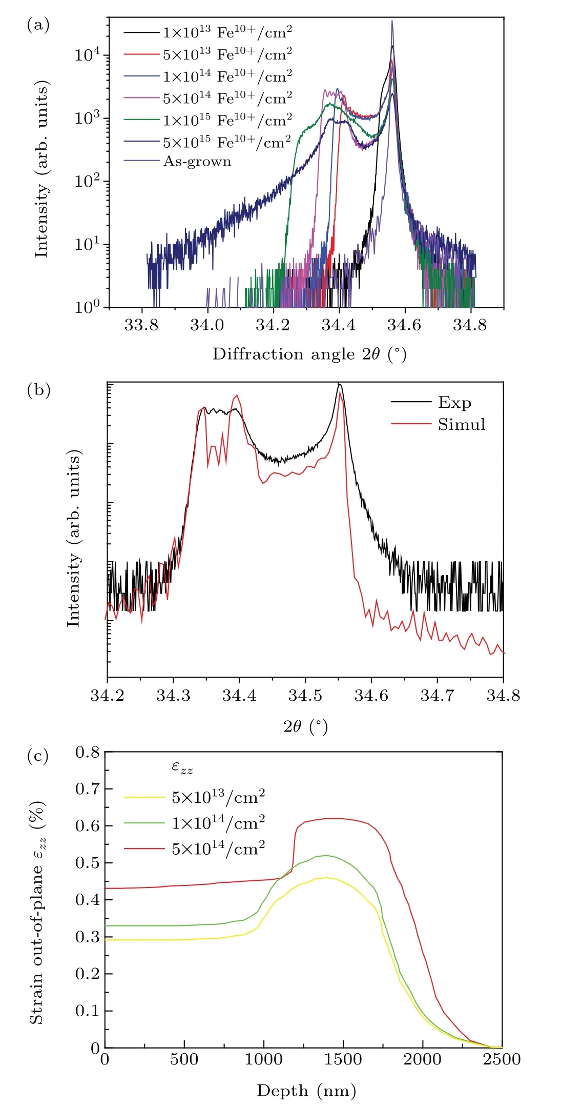
Fig.3. X-ray scattered intensity measurements along the surface normal direction close to the(0002)reflections in GaN implanted with 3-MeV Fe10+ions to fluences ranging from 1×10¹³ ions/cm2 to 5×10¹⁵ ions/cm2 at RT.The plot(b)shows a good agreement between experimental(Exp)and simulated(Simul)diffraction patterns for fluence 5×10¹⁴ ions/cm2. (c)Normal strain profiles in GaN implanted to different fluences change with depth.
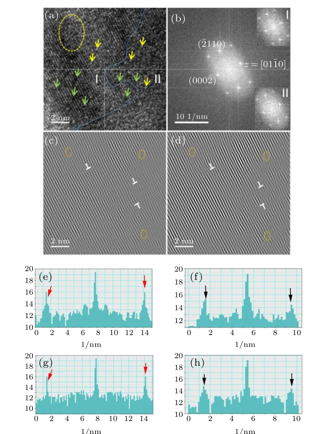
Fig.4. (a)HRTEM micrograph of the atomic configuration in the damaged layer where an amorphous zone is indicated by a yellow circle, and Ga vacancies and Ga interstitials are indicated by blue arrows and yellow arrows,respectively,as well as two different periodic lattices are presented in zones I and II, (b) FFT of HRTEM micrograph and insets taken from zones I and II,(c)IFFT of HRTEM micrograph, (d)IFFT of(0002)spots in panels(b),(e)to(h)intensity profiles extracted from the FFT pattern: (e)and(g)(¯2110)and (2¯1¯10) diffraction spots indicated by red arrows, (f)and (h) (0002) and(000¯2) diffraction spots indicated by black arrows where panels (e) and (f)are taken from zone I,and panels(g)and(h)are taken from zone II.
The formation of basal stacking faults is well recognized in GaN. The stacking fault formation energies are relatively low, so stacking faults are easily formed after ion implantation.[26,27]In our recent report of Xe-irradiated GaN,few perfect edge dislocations on the basal plane and abundant lattice distortion on the prism and pyramidal planes were found.[26]The damage process is that interstitials initially migrate and/or accumulate on the basal plane to form a basal stacking fault. It can be seen that some Ga atoms enriched or escaped on the basal plane,as indicated by arrows in Fig.4(a).The accumulation of Ga atoms on the(0001)plane leads to the formation of in-plane compressive stress and a positive strain out-of-plane. The evolution of the positive strain out-of-plane with irradiation fluence has been illustrated in Fig. 3(c). In order to release the positive strain out-of-plane, the atoms on the prism and pyramidal planes flow occur.[26]With further increase in lattice disorder,amorphous structure will be formed gradually.
4. Conclusion
In the present study,the chemical disorder on the surface,lattice strain,and atomic structure of GaN irradiated by Fe ions at RT have been investigated. The following conclusions are obtained. (i)The dissociation of Ga-N bonds due to ion sputtering, leads to the rapid oxidation of dangling bonds of Ga atoms. It should take care of surface reconstruction and surface chemical composite during ion implantation, in order to fabricate semiconductor devices. (ii)The profile of strain outof-plane with depth was obtained. The peak of the strain outof-plane is located at the maximum lattice disorder. The saturation of maximum strain after 5×10¹⁴-ions/cm2implantation was found. With further increase in fluence,lattice strain is released due to the formation of extended defects and amorphous structure. (iii)HRTEM characterization confirmed that interstitial-and vacancy-type stacking faults occurred initially on the basal plane. The Ga interstitials or Ga vacancies on the(0001)plane have been directly observed by HRTEM.Due to the lower displacement energy compared to Ga sublattice, N sublattice disorder also occurred.
Acknowledgments
Project supported by the National Natural Science Foundation of China (Grant No. 12075194) and the Fund of Collage Student Innovation and Entrepreneurship Training Program(Grant No.S202010619053). We appreciate the staff in the 320-kV high-voltage platform in the Institute of Modern Physics,Chinese Academy of Sciences for their assistance in ion implantation experiment.
猜你喜欢
华声文萃(2022年6期)2022-07-05
文萃报·周二版(2022年16期)2022-04-23
卫星应用(2022年1期)2022-03-09
小学生学习指导(低年级)(2021年10期)2021-11-01
音乐天地(音乐创作版)(2021年7期)2021-10-13
趣味(语文)(2020年5期)2020-11-16
青年歌声(2019年9期)2019-09-17
文学少年(原创儿童文学)(2019年3期)2019-05-23
读者(2017年8期)2017-03-29
军营文化天地(2017年2期)2017-03-08
- Chinese Physics B的其它文章
- Quantum walk search algorithm for multi-objective searching with iteration auto-controlling on hypercube
- Protecting geometric quantum discord via partially collapsing measurements of two qubits in multiple bosonic reservoirs
- Manipulating vortices in F =2 Bose-Einstein condensates through magnetic field and spin-orbit coupling
- Beating standard quantum limit via two-axis magnetic susceptibility measurement
- Neural-mechanism-driven image block encryption algorithm incorporating a hyperchaotic system and cloud model
- Anti-function solution of uniaxial anisotropic Stoner-Wohlfarth model