
Self-screening of the polarized electric field in wurtzite gallium nitride along[0001]direction
2022-04-12 03:45QiuLingQiu丘秋凌ShiXuYang杨世旭QianShuWu吴千树ChengLangLi黎城朗QiZhang张琦JinWeiZhang张津玮ZhenXingLiu刘振兴YuanTaoZhang张源涛andYangLiu刘扬
Chinese Physics B 2022年4期
关键词:张琦
Qiu-Ling Qiu(丘秋凌) Shi-Xu Yang(杨世旭) Qian-Shu Wu(吴千树)Cheng-Lang Li(黎城朗) Qi Zhang(张琦) Jin-Wei Zhang(张津玮)Zhen-Xing Liu(刘振兴) Yuan-Tao Zhang(张源涛) and Yang Liu(刘扬)
1School of Electronics and Information Technology,Sun Yat-Sen University,Guangzhou 510275,China
2States Key Laboratory of Integrated Optoelectronics,College of Electronic Science and Engineering,Jilin University,Changchun 130012,China
Keywords: gallium nitride,polarized electric field,self-screening effect,surface states,donor doping,intrinsic thermal excitation
1. Introduction
High-density two-dimensional electron gas (2DEG)could be induced by the strong spontaneous and piezoelectric polarization in wurtzite GaN materials.[1]It is widely used in the manufacture of high electron mobility transistors(HEMTs), Schottky diodes, Gunn diodes, and many other excellent radio frequency (RF) or power switching devices.Chaudhuriet al. used the negative polarization charges of GaN/Al(Ga)N interface to generate two-dimensional hole gas(2DHG)and formed a p-channel GaN HEMT with the lowest sheet resistance.[2]Simonet al.achieved high-conductivity ptype doping through polarization-induced technology, which improved the light emission efficiency in UV LEDs.[3]Combining with n-channel and p-channel GaN MOS-HEMTs structures on the same wafer, Chuet al. first demonstrated the GaN complementary metal-oxide-semiconductor(CMOS) field-effect-transistor technology. They successfully fabricated an integrated inverter and provided new feasibility for the GaN-integrated circuit.[4]In addition, Al-GaN/GaN HFETs,[5]MOSFETs,[6]GaN tunnel junction LEDs,[7]GaN polarization superjunction,[8]and many other high-performance devices were also developed using the polarization characteristics of GaN materials.
The polarization charges on the GaN surface generate the polarized electric field inside GaN. Carriers would be redistributed to compensate the polarized electric field.The process mentioned above is known as the self-screening effect. Zhanget al., Nanyang Technological University, first proposed the polarization self-screening effect. They demonstrate that the quantum confined Stark effect (QCSE) in LEDs can be selfscreened by bulk charges induced by InGaN quantum barrier with graded indium composition.[9]Mishraet al.,the University of California, has discussed the phenomenon of screening of polarized electric field in n-type GaN bulk materials with donor-like surface states and n-type impurities.[10]However, they did not systematically explain the self-screening effect and the origin of screening charges. So far, the selfscreening effect under the polarized electric field in GaN bulk materials has not been discussed in-depth and studied comprehensively. In this work, we used a combination of theoretical analysis and semiconductor technology computer-aided design (TCAD) simulations to study this effect. We systematically study the self-screening effect of the polarized electric field in GaN bulk materials under different situations such as ideal intrinsic GaN, intrinsic GaN with donor-like surface states,n-type GaN,and actual bulk GaN.After that,we clarify the source and accumulation of the screening charges caused by the self-screening effect. It can be considered that the essence of 2DEG in GaN is the accumulation of screening charges influenced by the self-screening effect of the polarized electric field. Therefore, this research will provide the accurate guidance for the structural design and the characteristic analysis of GaN devices.
2. TCAD experiment
The experimental conditions are determined by the following actual situations.
Wurtzite GaN has two polarities along thec-axis direction, Ga-polar and N-polar. The high densities of negative polarization charges and positive polarization charges are concentrated on the Ga-face and N-face of GaN material respectively. Ga-polar GaN epitaxy technology is more developed than N-polar GaN and the Ga-polar GaN-based devices have been put into commercial production and widely used. In order to be realistic,GaN bulk materials are all grown along with the [0001] direction in this paper. We assume that the ideal GaN bulk materials are relaxed, that is, there is only spontaneous polarization in GaN. If the spontaneous polarization intensityPspis 2.9×10⁻⁶C/cm-2,[11]the surface polarization charges densitynπwould be 1.8×1013cm-2.
GaN materials are generally grown on heterogeneous substrates[12,13]by MOCVD, MBE or HVPE. The material quality is greatly affected by growth parameters such as temperature,V/III ratio or the lattice parameters of heterogeneous substrates. So the concentration or density of the impurities,defects or surface states in GaN materials would generally be quite high.[14,15]Many studies have shown that actual GaN materials are n-type due to the existence of silicon doping,[16]oxygen impurity,[17,18]and surface states (such as nitrogen vacancies[19,20]). Therefore,in this work,we analyze the selfscreening effect of the polarized electric field in the ideal intrinsic Ga-face GaN bulk materials. Then intrinsic bulk GaN with donor-like surface states and with n-type doping are discussed respectively. Finally,we analyze a complex case about GaN bulk materials with both surface states and n-type doping. So that we could clarify the self-screening effect of the polarized electric field in an actual GaN bulk materials.
3. Result and discussion
The simplified symbols used in all figures are shown in Table 1, and the physical terms in all equations are described in Table 2.
Table 1. The definition of simplified symbols used in all figures.
Table 2. The physical terms defined or described in all equations.
3.1. Intrinsic GaN on Ga-face
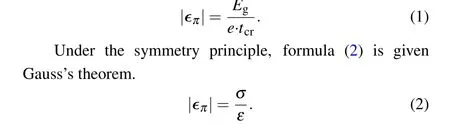
The direction ofεπin bulk GaN is from N-face to Gaface,and the intensity ofεπcan be calculated by Poisson equation:|επ|=nπ/ε ≈3.45 MV/cm.
If the polarization charges cannot be screened,there will be a strong constant polarized electric field of an order of MV/cm inside GaN, which slopes the energy band of GaN.There is a significant energy difference between the top of the Ga-face valence band and the Fermi level in thin bulk GaN. In this case, the intrinsic thermal excitation hardly occurs and its influence on the polarized electric field can be ignored. The electric field in GaN should be constant,as shown in Fig. 1(a). As the thickness of GaN increases, the energy difference between the top of Ga-face valence band and Fermi level gradually decreases.When the top of the Ga-face valence band is quite close or getting to the Fermi level,the probability of intrinsic thermal excitation increases sharply,and many electron-hole pairs are excited, as shown in Fig. 1(b). The electrons and holes drift to N-face and Ga-face respectively to screen a part of the polarized electric field. The total electric field inside the GaN reduces and the slope of energy band begins to decrease. With the thickness of GaN increasing further, like Fig. 1(c), the Fermi level is clamped at the Ga-face valence band. The intrinsic thermal ionization is promoted,excites more screening charges and the polarized electric field is getting screened further.
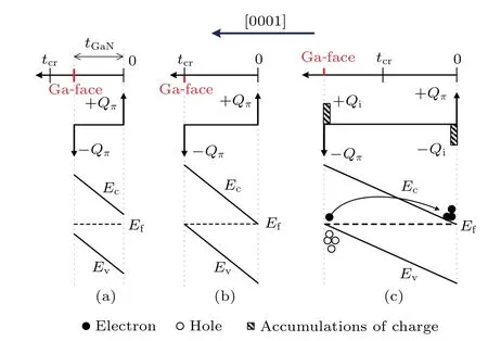
Fig.1. The material structure,charges block diagram,and energy band diagram during the epitaxial growth of intrinsic bulk GaN:(a)the case when tGaN is less than tcr, (b) the case when tGaN is equal to tcr, and (c) the case when tGaN is greater than tcr.
When the Ga-face valence band is equal to the Fermi level,the GaN thickness is called the critical thickness of GaN.In this case, assuming that the intensity of the polarization electric field is almost constant, the uniform electric field intensity in GaN should be approximately equal to
Combining formulas (1) and (2), thetcrcan be approximately considered to be related to the material’s bandgap and the intensity of polarized electric field[10]
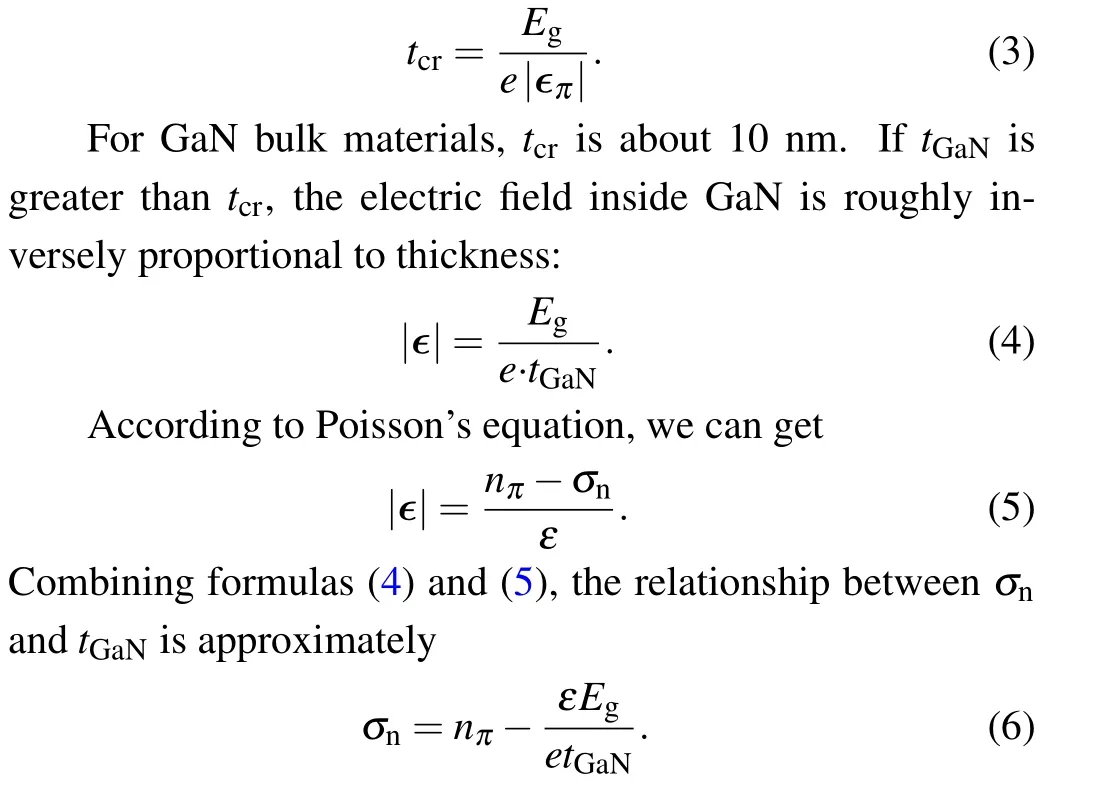
We simulate intrinsic GaN bulk materials with different thicknesses by TCAD simulations. The energy band of intrinsic bulk GaN is shown in Fig.2(a)and it is basically the same as our analysis. TheEfis clamped at the Ga-face valence band and the N-face conduction band.The carrier distribution in the 3-µm bulk GaN is extracted and shown in Fig.2(b), and it is also consistent with our analysis.
Theσnand intensity ofεobtained by simulations are compared with theoretical analysis results,as shown in Fig.3.The error is less than 5% aboutσnand less than 15% aboutε. Figure 3(a)shows theεandσnas a function of GaN thickness. It can be found that as thetGaNincreases,σngradually increases, which promotes the screening of polarized electric field. So that the net charges on the Ga-face and N-face of the GaN decreases and then the internal electric field decreases.It is worth noticing that althoughσnis close to thenπ, it still cannot fully compensate the polarization charges. Figure 3(b)shows that as the bulk GaN thickness increases from 10 nm to 10 µm, Ga-face net charge density reduces from 1.8×1013cm-2to 4.1×1010cm-2, and electric field intensity reduces from 3.4 MV/cm to 3 kV/cm but the∊πis still not completely screened.
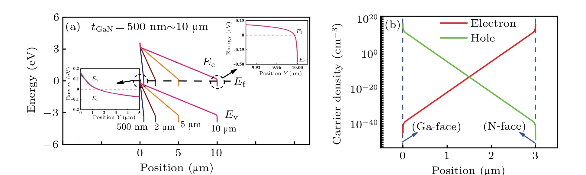
Fig.2. (a)Band diagram of 500 nm-10µm GaN,(b)spatial distribution of charges in 3-µm GaN bulk material.
Fig. 3. Comparison of theoretical results of the self-screening effect of the polarized electric field in intrinsic bulk GaN with the TCAD simulation results. (a)The relationship between the screening charge density and the electric field of the GaN material as a function of GaN thickness,(b)Ga-face net charge density as a function of GaN thickness.
3.2. Intrinsic GaN with Ga-face donor-like surface states
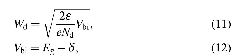
The self-screening effect of the polarized electric field in intrinsic GaN with Ga-face donor-like surface states is like that in intrinsic bulk GaN. As a thin GaN, a large energy difference is between the surface state energy level and Fermi level.The ionization probability of the donor-like surface states is extremely low, as shown in Fig. 4(a). AstGaNincreases, the difference betweenEDDand Fermi level gradually decreases.Whenδis small enough, the probability of donor-like surface state ionization increases and electrons are ionized to screen a part of the polarized electric field, leaving positive ionized donor-like surface states,as shown in Fig.4(b). Analogously, when Ga-face Fermi level is equal toEDD, we call this GaN thickness as the critical thickness. Same method as formula(3),thetDDcrapproximately depends onEDD,
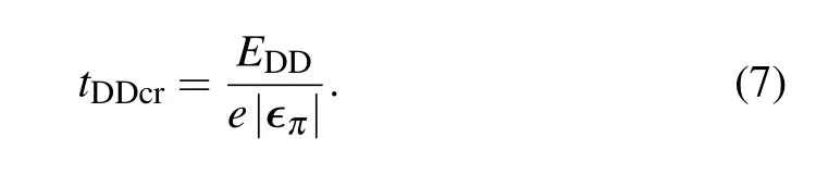
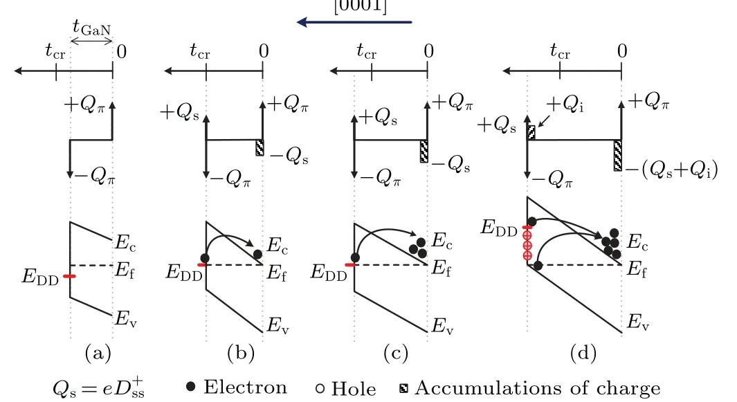
Fig.4. The material structure,charges block diagram,and energy band diagram of intrinsic bulk GaN with Ga-face donor-like surface states: (a)the case when tGaN <tDDcr, (b) the case when tGaN =tDDcr, (c) the case when tGaN >tDDcr and Dss >ns-cr,(d)the case when tGaN >tDDcr,but Dss <ns-cr.
WhentGaNis greater thantDDcr, the Fermi level will be clamped atEDD. The Ga-face donor-like surface states will be further ionized,more electrons will be ionized and concentrate on N-face to screen polarized electric field, as shown in Fig.4(c). However,whenDssis less thannπ,with the increase oftGaN,the intrinsic thermal excitation occurs after the donorlike surface state is completely ionized and continues to screen polarized electric field. So,the Fermi level will be clamped at Ga-face valence band instead ofEDD, as shown in Fig. 4(d).Therefore, with a certaintGaN(greater thantDDcr) andEDD,there is a critical donor-like surface state density resulting in the Fermi level being clamped at the transition fromEDDto Ga-face valence band. From formula (6) the specific mathematical relationship ofns-crin this case is

We simulated the GaN bulk material with Ga-face donor-like surface states and the energy band of 3-µm GaN with differentDssatEDD=1 eV.[21]The results are shown in Fig.5(a).WhenDssis higher than 5×1013cm-2, the Fermi level is always clamped atEDD. WhenDssis lower than 1×1013cm-2,the Fermi level is always clamped at the Ga-face valence band. That means thens-cris between 1×1013cm-2and 5×1013cm-2.Figure 5(b)shows thens-crunder differenttGaNandEDD.Thens-crshows a decreasing trend with the increase of the donor energy level. As GaN thickness increases,ns-crgradually approachesnπ. These results are consistent with our theoretical analysis.

Fig.5. (a)Energy band diagrams of bulk GaN with different Dss,(b)the corresponding ns-cr at different tGaN and EDD.
3.3. The n-type GaN without surface states
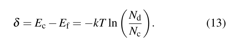
For bulk GaN with only n-type doping, the electrons are ionized by impurities and directionally drift to the N-face of GaN under the polarized electric field,leaving the positive ionized impurities which forms a depletion region,playing a certain role in screening polarized electric field. IftGaNis greater thantcr, the surface potential (φs) of GaN can be considered approximately equal toEg,and theWdshould be
Combining formulas (11)-(13), theWdformed by donor impurity ionization is mainly affected byNdandVbi,but not by GaN thickness. AsNbincreases,the bottom of the conduction band gets closer to the Fermi level. It is worth noticing that althoughNbis quite low(1015cm-3in our simulations and calculations),δis only about 0.2 eV,calculated by formula(13),which is negligible compared withEg(about 3.4 eV).So that the formula(11)can be approximated as
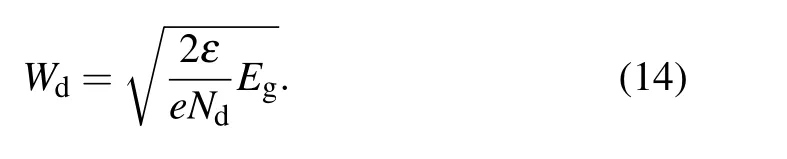
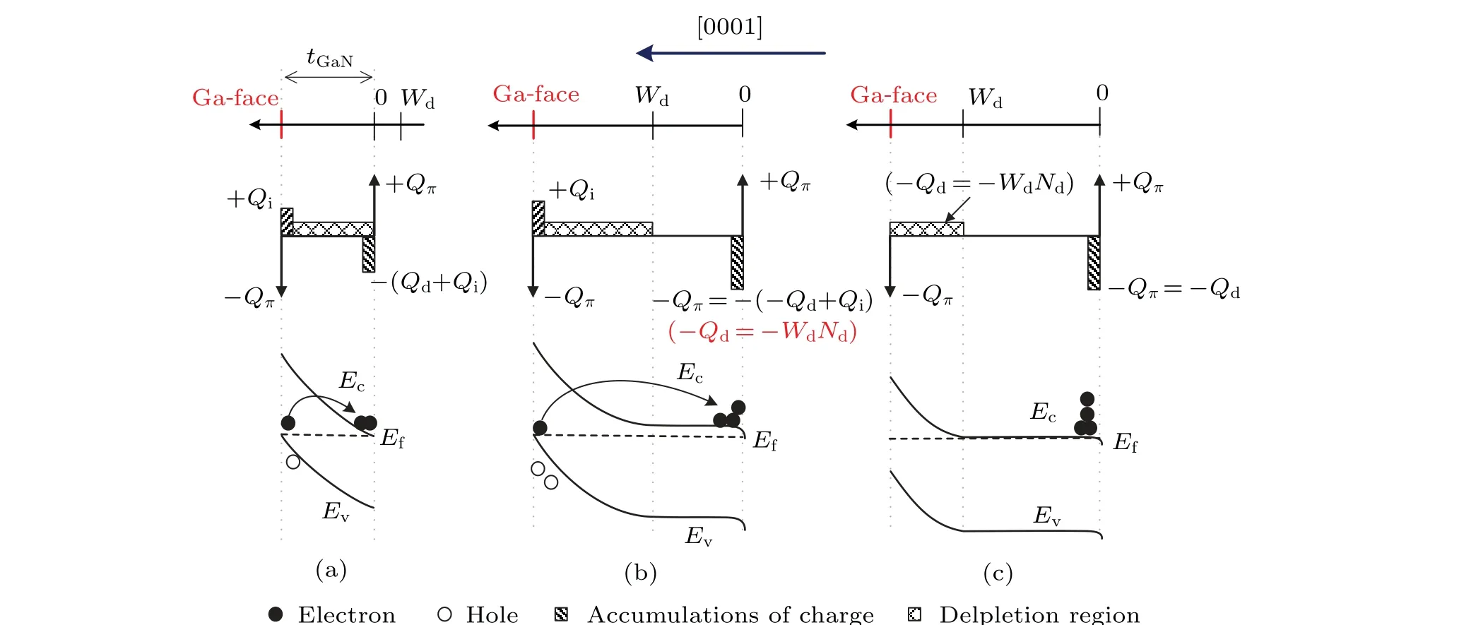
Fig.6. The material structure,charges block diagram,and the energy band diagram of bulk GaN with donor impurities: (a)the case when tGaN <Wd,(b)the case when tGaN >Wd and Nd <1019 cm-3,(c)the case when tGaN >Wd and Nd ≥1019 cm-3.
By further analysis we know that iftGaNis less thanWd,the donor impurity in the GaN material will be completely ionized,as shown in Fig.6(a). The screening charge density provided isNd·tGaN,which should be less thannπ. In this case,a part of screening charges should be provided by intrinsic thermal excitation, so that the Fermi level will be clamped at the Ga-face valence band. AstGaNincreases to be greater thanWd, a flat energy band region appears, which means that the polarized electric field is completely screened in that region like Fig. 6(b). Figure 6(b) shows a condition about theNdis lower than 1019cm-3(a critical value ofNdin our simulation. WhenNdis 1019cm-3,the electron density provided by donor impurity ionization is exactly equal tonπin Fig.7(a)),the electron density provided by donor impurity ionization isNd·Wdand it is still less thannπ. So that the Fermi level is clamped at the Ga-face valence band to complement screening charges. However, whenNdis greater than or equal to 1019cm-3, the electron density provided by donor impurity ionization is already greater thannπ. Due to the self-stability of charges in a balanced system,the Fermi level would not be clamped at the Ga-face valence band and no obvious intrinsic thermal excitation occurs. TheWdwill also decrease because theφsof GaN decreases, ensuringNd·Wdis exactly equal tonπ. In this case,the polarized electric field inside GaN would be completely screened and the internal energy band gets flat,as shown in Fig.6(c).
Figure 7(a) shows the energy band characteristics of bulk GaN with various donor doping concentrations from 1015cm-3to 1019cm-3obtained by TCAD simulations.With the increase ofNd,Wdgradually decreases. The flat region of the energy band indicates that the electric field is 0 and the polarized electric field is completely screened. AsNdis about 1015cm-3-1018cm-3, the Fermi level is clamped at the Gaface valence band. WhenNdis equal to 1019cm-3,the Fermi level is no longer clamped at the Ga-face valence band.
Figure 7(b) shows the electron density provided by the donor impurity ionization,total screening charge density,andWdfrom simulation and theoretical analysis results. With the increase of the doping concentration,σngradually increases,while the remaining electrons provided by intrinsic thermal excitation gradually decreases and the total screening charge density is still equal tonπ,which means the polarized electric field inside GaN is always completely screened.
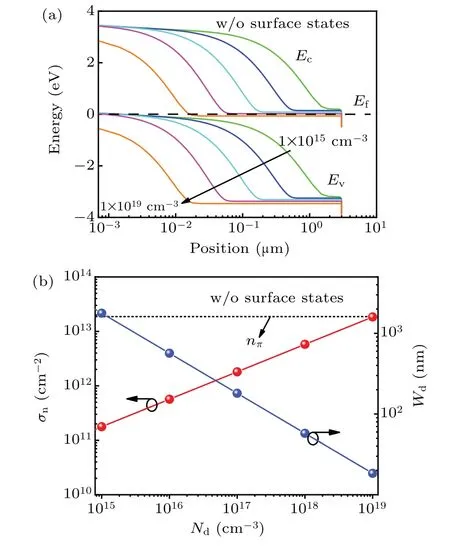
Fig.7. (a)Energy band diagram of bulk GaN with different n-type doping concentrations (semi-logarithmic coordinates), (b) σn and Wd provided by donor impurity ionization under different doping concentrations.
3.4. The n-type GaN without surface states
Generally, there are both donor-like surface states and shallow-level donor impurities[21]in actual GaN materials,and the two factors together impact the polarized electric field inside GaN. TheWdis generally from tens of nanometers to several microns and thetDDcris only several nanometers,which is much smaller thanWd. IftGaNis less thantDDcr,the charges from impurity ionization,donor-like surface states ionization, and intrinsic thermal excitation together still cannot completely screen the polarized electric field, the energy band characteristics would be just like Fig.4(a)and have little practical significance. So,the following analysis assumes that the thickness of GaN is always greater thantDDcr.
WhenDssis greater thanns-cr, Fermi level will be clamped atEDD, as shown in Figs.8(a)and 8(b). WhentGaNis less thanWd, as shown in Fig. 8(a) and donor impurities are completely ionized but cannot completely screen the polarized electric field. ThetGaNin Fig.8(b)is greater thanWdand a part of donor impurities are ionized. The electrons from donor impurities and donor-like surface states screen the polarized electric field and form a flat energy band region. The screening charges in Figs. 8(a) and 8(b) come from ionizing donor impurities and donor-like surface states.
AsDssis less thanns-cr, donor-like surface states are completely ionized and the Fermi level is clamped at Ga-face valence band,which means a part of screening charges are provided by intrinsic thermal excitation like Figs. 8(c) and 8(d).Like the analysis above, figure 8(c) shows that whentGaNis less thanWd,the donor impurities are completely ionized and the polarized electric field cannot be completely screened.Figure 8(d)shows that whentGaNis greater thanWd,the polarized electric field is completely screened and a flat energy band region appears. The screening charges in Figs. 8(c) and 8(d)come from ionization of donor impurities, donor-like surface states,and intrinsic thermal excitation which is different from the case in Figs.8(a)and 8(b).
Generally,in GaN with both donor-like surface states and donor impurities, the density of the donor-like surface states first determines the position where the Fermi level is clamped and theVbi. Then it determines theWdand the density of screening charges that can be provided.The sources of screening charges are summarized in Fig. 9. IftGaNis greater thanWd, the polarized electric field can be completely screened.The sources of screening charges mainly include the electrons provided by the ionization of the donor-like surface states and the donor impurity ionization. When the surface state density is low,the intrinsic thermal excitation occurs and provides screening charges. But iftGaNis greater thanWdand heavily doped(over 1019cm-3),the intrinsic thermal excitation would rarely occur.That case can be comprehended uncomplicatedly following the analysis in Subsection 3.3,Fig.6(c).
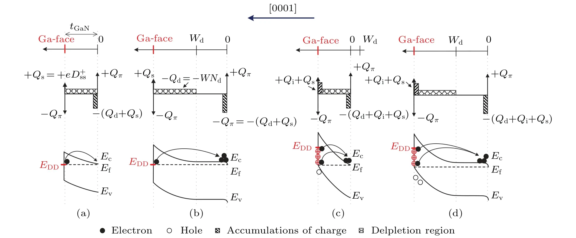
Fig.8. The material structure,charges block diagram,and energy band diagram of bulk GaN with both donor-like surface states and donor impurities:(a) the case when Dss >ns-cr, tGaN <Wd, and Nd <1019 cm-3; (b) the case when Dss >ns-cr, tGaN >Wd, and Nd <1019 cm-3; (c) the case when Dss <ns-cr,tGaN <Wd,and N ≥1019 cm-3;(d)the case when Dss <ns-cr,tGaN >Wd,and N ≥1019 cm-3.
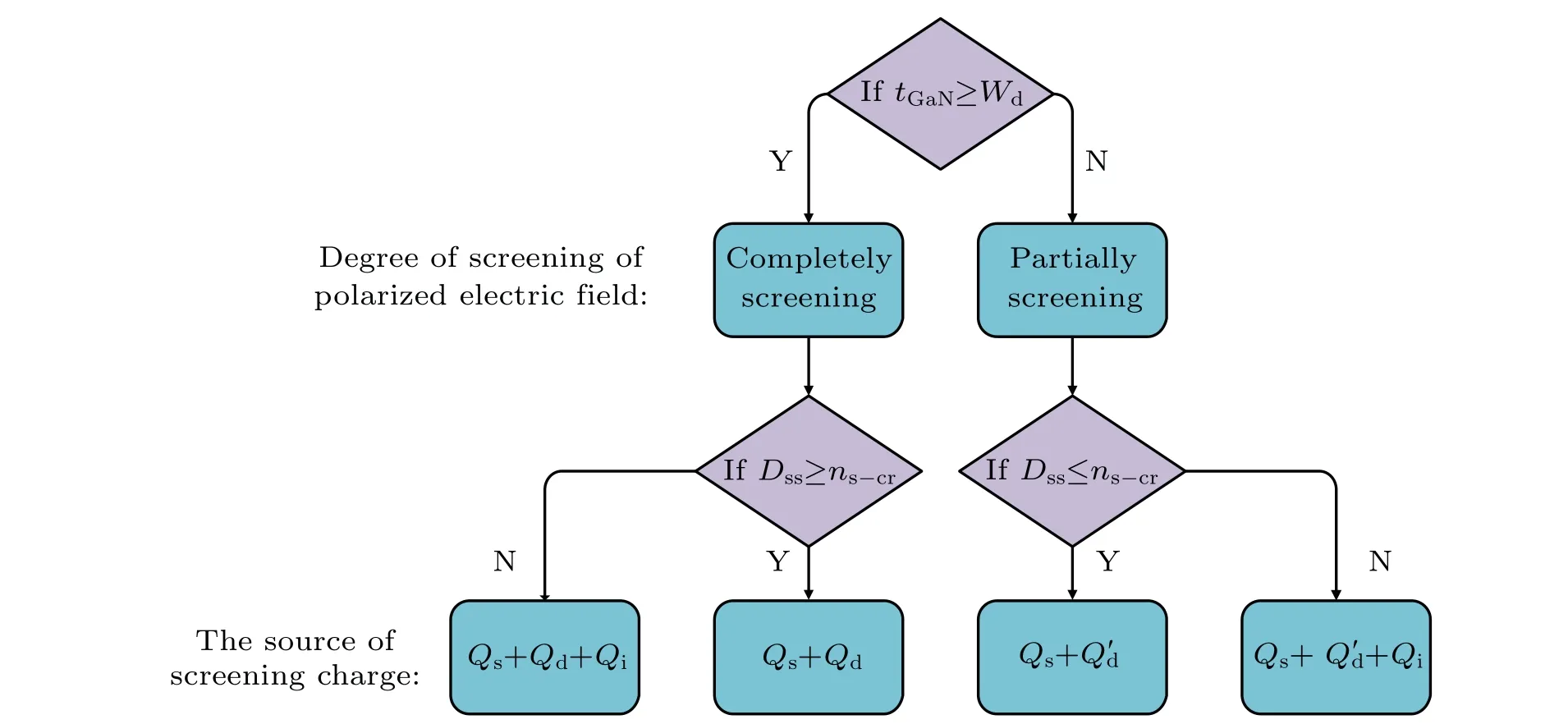
Fig. 9. The source of screening charges in bulk GaN. In the figure, Q'd is the screening charges provided by the ionization of donor impurities when tGaN <Wd and Q'd=tGaN·Nd.
For GaN with various values ofDssandNd, figure 10 shows their TCAD simulation results of the band structure.ThetGaNis greater thanWdin simulations. The energy band has a flat region and the polarization electric field is completely screened. WhenDssis 1014cm-2, the Fermi level is clamped atEDD,the built-in potential should beVbi=EDD-δin this condition. TheWdand electron density provided by donor impurity ionization are determined byVbi. The remaining electrons are provided by the ionization of the donor-like surface states. WhenDssis 1013cm-2, the Fermi level is clamped at the Ga-face valence band and the built-in potential should beVbi=Eg-δin this condition. Donor-like surface states are completely ionized and the remaining electrons are provided by donor impurity ionization and intrinsic thermal excitation, which can be seen to be consistent with our theoretical analysis.

Fig. 10. Energy band diagram of bulk GaN with both donor surface states and donor impurities.
4. Conclusion and perspectives
In summary, this work uses TCAD simulations to study the self-screening effect of the polarized electric field in Gaface bulk GaN and the source of screening charges with several conditions: (i) The electric field in intrinsic bulk GaN is inversely proportional to GaN thickness,screening charges provided by intrinsic thermal excitation.(ii)In intrinsic GaN with Ga-face donor-like surface states,there is a critical donor-like surface state density which decides where the Fermi level is clamped. And it determines the density of screening charges and the degree of screening of the polarized electric field in GaN.(iii)In bulk GaN with donor impurities,if GaN thickness is greater than the width of the depletion region,the polarized electric field inside the GaN can be completely screened. In this condition, the screening charges are provided by donor impurity ionization and intrinsic thermal excitation. However,they are only provided by donor impurity ionization when GaN is heavily doped. (iv)As GaN with both Ga-face donorlike surface states and donor impurities,only when the thickness of GaN is greater than the width of the depletion region,can the polarization electric field in GaN be completely screened. And the donor-like surface state density determines the surface potential of the GaN,determining the width of the depletion region and density of screening charges provided by donor impurities in that condition. The sources of screening charges are mainly donor impurity ionization and donorlike surface states ionization. The intrinsic thermal excitation could participate in the screening effect when the surface state density is lower than the critical value.
Acknowledgement
Project supported by the Key Research and Development Program of Guangdong Province, China (Grant No.2020B010174003).
猜你喜欢
科学与财富(2021年36期)2021-05-10
现代信息科技(2021年21期)2021-05-07
党员文摘(2020年6期)2020-07-16
廉政瞭望·下半月(2020年3期)2020-05-26
杂文选刊(2020年4期)2020-04-19
文萃报·周五版(2020年13期)2020-04-07
中国新闻周刊(2019年34期)2019-09-20
风流一代·青春(2018年10期)2018-10-18
美与时代·城市版(2017年3期)2017-05-19
中国民族民间医药·上半月(2017年2期)2017-03-09
- Chinese Physics B的其它文章
- Quantum walk search algorithm for multi-objective searching with iteration auto-controlling on hypercube
- Protecting geometric quantum discord via partially collapsing measurements of two qubits in multiple bosonic reservoirs
- Manipulating vortices in F =2 Bose-Einstein condensates through magnetic field and spin-orbit coupling
- Beating standard quantum limit via two-axis magnetic susceptibility measurement
- Neural-mechanism-driven image block encryption algorithm incorporating a hyperchaotic system and cloud model
- Anti-function solution of uniaxial anisotropic Stoner-Wohlfarth model