
Thermoelectric performance of XI2(X =Ge,Sn,Pb)bilayers
2022-04-12 03:47NanLu陆楠andJieGuan管杰
Chinese Physics B 2022年4期
Nan Lu(陆楠) and Jie Guan(管杰)
School of Physics,Southeast University,Nanjing 211189,China
Keywords: 2D group-IV diiodide,thermoelectric materials,bilayers
1. Introduction
High quality thermoelectric (TE) materials and their applications have provided an effective way for the transforming from heat to electricity and received intense researches for the significant contributions to the global sustainable energy solution.[1-4]Traditionally, the efficiency of TE materials is measured primarily by the dimensionless figure of merit,ZT,defined as[1,5]ZT=S2σT/(κL+κe), whereS,σ,T,κL,κeare the Seebeck coefficient, electrical conductivity, absolute temperature, lattice thermal conductivity, and electrical thermal conductivity,respectively. In terms of the formula ofZT,high Seebeck coefficient,high electrical conductivity,and low thermal conductivity are required to enhance the TE performance.
Conventionally, increasing the electrical power factor(PF=S2σ) and reducing theκLare two general approaches to obtain high-quality TE materials. Regarding increasing thePF, one successful way is to get a large density of states(DOS) effective mass by converging the valence (or conduction)bands.[6]Various strategies such as alloying,[7]elemental doping,[8]and strain engineering[9,10]have been developed to achieve the convergence of the bands and consequently to improve the TE performance. For the reduction ofκL, it is an effective strategy to enhance the phonon scattering by introducing multiscale scattering centers,e.g., point-defects[11,12]or grain boundaries.[13]However,suppressingκLthrough the phonon engineering is actually difficult to achieve without simultaneously affecting electron transport.[6]Hence, seeking new materials with intrinsically high power factor and low thermal conductivity is a preferable approach to obtain high TE performance.
In 1993, the seminal work of Hicks and Dresselhaus showed that reducing the dimension of the system could significantly increaseZTvalue, due to the enhancedPFcaused by an increased DOS near the Fermi level and the reducedκLcaused by the increased phonon scattering from the surface.[2,14]With the emerging field of layered materials in the past decades, a number of investigations have been conducted on two-dimensional (2D) TE materials, such as SnSe,[15]SnTe,[16]GeTe,[17]SiTe,[18]XSb (X= Si, Ge,Sn),[19]phosphorene,[20,21]and transition metal dichalcogenides (TMDs).[22-24]Recently, the 2D group-IV diiodide family, including PbI2, GeI2, SnI2, and SiI2, have shown excellent thermoelectric performance.[25-27]Theoretical results showed that the maximumZTvalue is 4.04 at 600 K for GeI2monolayer[26]and is 4.9 at 900 K for PbI2monolayer,[25]which are better than the well-known TMDs and other 2D materials. On the other hand, it is well known that the physical properties of 2D materials are sensitive to inter-layer interaction[28]and in experiment, it is not easy to obtain the monolayer for most 2D materials. Thus,it is intriguing to explore the TE performance for the multilayers of 2D group-IV diiodides.
In this work, by combiningab initiodensity functional theory (DFT) with the Boltzmann transport theory, we compared the electrical and thermal transport properties between the monolayers and bilayers of 2DXI2(X= Ge, Sn, Pb).Phonon spectra have been calculated to confirm the dynamical stability of all the 2DXI2structures. TheκL,group velocity(Vg),and phonon lifetime(τph)were calculated and the results show that theκLat room temperature for the bilayers are about 1.6 times as large as the corresponding monolayers for all the three materials, which is possibly caused by the largerτphfor bilayer. Both acoustic and optic phonon modes contribute to the thermal conductivity as a result of the relatively low frequency of the optical phonon modes. Electronic structure was investigated and all the monolayer and bilayer structures are shown to be semiconducting with an indirect band gap close to 2 eV.Carrier mobility(µ)and relaxation time(τ)were also calculated to further explore the electrical transport properties. Finally, the values of theS,σ,PF, andZTalong different directions were compared between the monolayers and bilayers ofXI2. The results show that for all the threeXI2structures,the bilayers display much less direction-dependent TE efficiency and have much larger n-typeZTvalues compared with the monolayers. The dramatic difference between the monolayer and bilayer indicates that the inter-layer interaction plays an important role in the TE performance ofXI2,which provides an effective tunability on their TE characteristics.
2. Theoretical method
The lattice thermal transport properties can be calculated based on the phonon Boltzmann transport equation(BTE)and the interatomic force constant (IFC) obtained from DFT calculations. The lattice thermal conductivity alongαdirection is defined as[29]
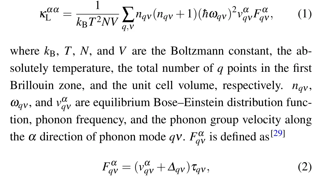
whereτqνis the phonon relaxation time of modeqν. All the calculations are carried out with the DFT method, as implemented in the Viennaab initiosimulation package(VASP).[30]We choose the generalized gradient approximation (GGA) in the Perdew-Burke-Ernzerhof (PBE) parametrization for the exchange-correlation functional. To avoid the interactions between adjacent layers, the vacuum region is set in excess of 20 °A.The cutoff energy is set as 500 eV for the plane wave basis. A 9×9×1k-mesh is used during structural relaxation for the unit cell until the energy differences are converged within 10-6eV,with a Hellman-Feynman force convergence threshold of 10-3eV/°A.
The lattice thermal conductivity is calculated by solving the BTE implemented with a fully iterative self-consistent program in ShengBTE package.[31]When using ShengBTE, the 2nd-order (harmonic) and the 3rd-order (anharmonic) IFCs matrixes are required. The harmonic IFCs are obtained using density functional perturbation theory, which calculates the dynamical matrix through the linear response of electron density.[32]The 5×5×1 supercell with 3×3×1k-mesh is used to ensure the convergence. The phonon dispersion is obtained using the Phonopy code.[33]Besides the harmonic IFCs mentioned above, the 4×4×1 supercell and 3×3×1k-mesh are used to obtain the anharmonic IFCs, and an interaction range including the forth-nearest-neighbor atoms is considered. TE properties were computed by solving the BTE under a constant relaxation timeτand a rigid band approximation performed in the BoltztraP2 code.[34]The Seebeck coefficientSand electrical conductivityσcan be obtained by investigating the electronic transport properties based on DFT calculations and the integration of the transport distributionΞ(ε)=∑k vk ⊗vkτk[35]
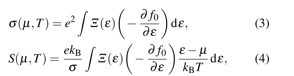
wheref0is the equilibrium Fermi-Dirac distribution function,kBis the Boltzmann constant, andµis the chemical potential. Thevkandτkare the group velocity and relaxation time at statek, respectively. We used a very densek-point mesh of 60×60×1 to obtain a convergent density of states. The electrical conductivity(σ/τ)we obtained is dependent on the carrier relaxation timeτ. The electronic thermal conductivityκeis calculated using the Wiedemann-Franz law,κe=LσT,
whereLis the Lorenz number. Here,we use the Lorenz number of 1.5×10⁻⁸W·Ω·K-1.[36]
3. Results and discussion
The equilibrium structures for the monolayers and bilayers ofXI2are shown in Fig.1. The monolayers exhibit buckled sandwich hexagonal crystal structure with the space group of 164 (P-3m1). There are oneXatom and two I atoms in a unit cell. Our DFT calcultaions show that the lattice constants are 4.30 °A,4.57 °A,and 4.66 °A for GeI2,SnI2,and PbI2,respectively, which are in good agreement with previous reported values.[37,38]For all the threeXI2bilayers,AA-stacking is found energetically preferable. The inter-layer distances are respectively 7.75 °A, 7.67 °A, 7.86 °A in GeI2, SnI2, and PbI2.The obtained inter-layer binding energies for all theXI2bilayers are less than 0.01 eV/atom at PBE level,which indicates a typical van der Waals(vdW)interaction.

Fig.1.Ball and stick model for the equilibrium structures of an XI2(X=Ge,Sn,Pb)(a)monolayer and(b)bilayer. Both top and side views are shown.The X and I atoms are shown in green and mauve balls, respectively. d is the inter-layer distance in the bilayer. The primitive cell in the top view is denoted by the red shadow.
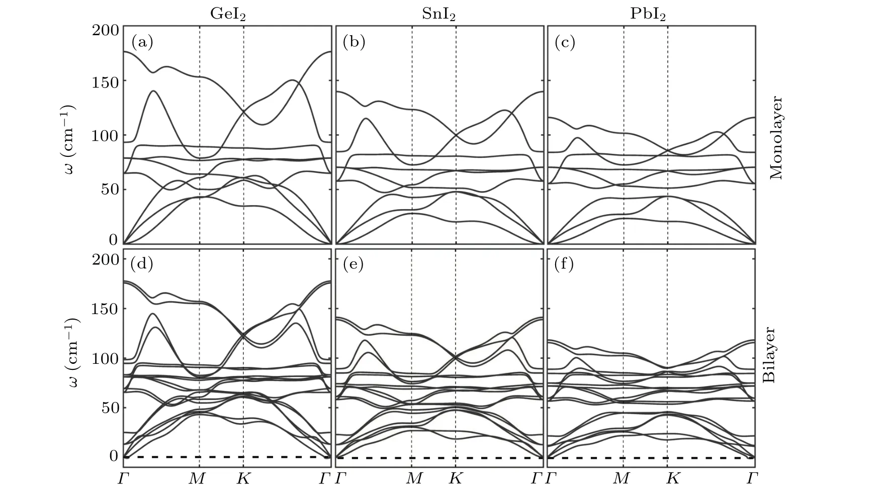
Fig.2. Phonon dispersion in the first Brillouin zone for the monolayer(upper panel)and bilayer(lower panel)of[(a),(d)]GeI2,[(b),(e)]SnI2 and[(c),(f)]PbI2,respectively.
Based on the phonon Boltzmann transport equation(BTE) and the interatomic force constant (IFC), we calculated theκLof theXI2structures using the iterative method in ShengBTE code.[31]As the results plotted in Fig.3,κLdecreases as temperature increases and the values for the monolayers at 300 K reach 1.14 W·m-1·K-1, 0.78 W·m-1·K-1,and 0.63 W·m-1·K-1for GeI2, SnI2, and PbI2, respectively.Our results of GeI2and PbI2are consistent with previously reported theoretical results.[26,41]The values ofκLfor the bilayers(1.74 W·m-1·K-1,1.25 W·m-1·K-1,1.05 W·m-1·K-1for GeI2,SnI2,PbI2at 300 K,respectively)are about 1.6 times as large as that for the monolayers but still at a relatively low level,which ensures their high TE efficiency.Our results of the low in-planeκLfor PbI2monolayer and bilayer are also reasonably consistent with the experimental results of the crystalline PbI2(0.681 W·m-1·K-1at 300 K)[42]and the relatively low Debye temperature estimated by the experimentally measured temperature-dependent band gap values.[43]What is more, the values ofκLare found decreasing in order of the increasing atom mass from Ge to Pb,which is consistent with the phonon dispersion results discussed above.
The group velocity and the phonon lifetime have been calculated to further explore the internal physical mechanism of the intrinsically lowκLof theXI2layers. TheVgof each phonon mode is calculated based on the second-order (harmonic) interatomic force constants. As shown in Figs. 4(a)-4(c),the monolayers and bilayers have similar distributions ofVgfor all theXI2structures. In general,theVgdecreases with the atomic mass increasing from Ge, Sn to Pb, indicating the decreasingκLfrom GeI2to PbI2. Conventionally,the acoustic modes at the low frequency dominate the thermal conductivity,which is because the optical modes have relatively low group velocities and hard to be excited for their high frequency.[44-46]In our investigated case,however,the low vibration frequency of the optical phonon modes causes their involvements in the low frequency thermal transport. Thus, all theXI2structures have comparable values ofVgfor acoustic and optic phonon modes.
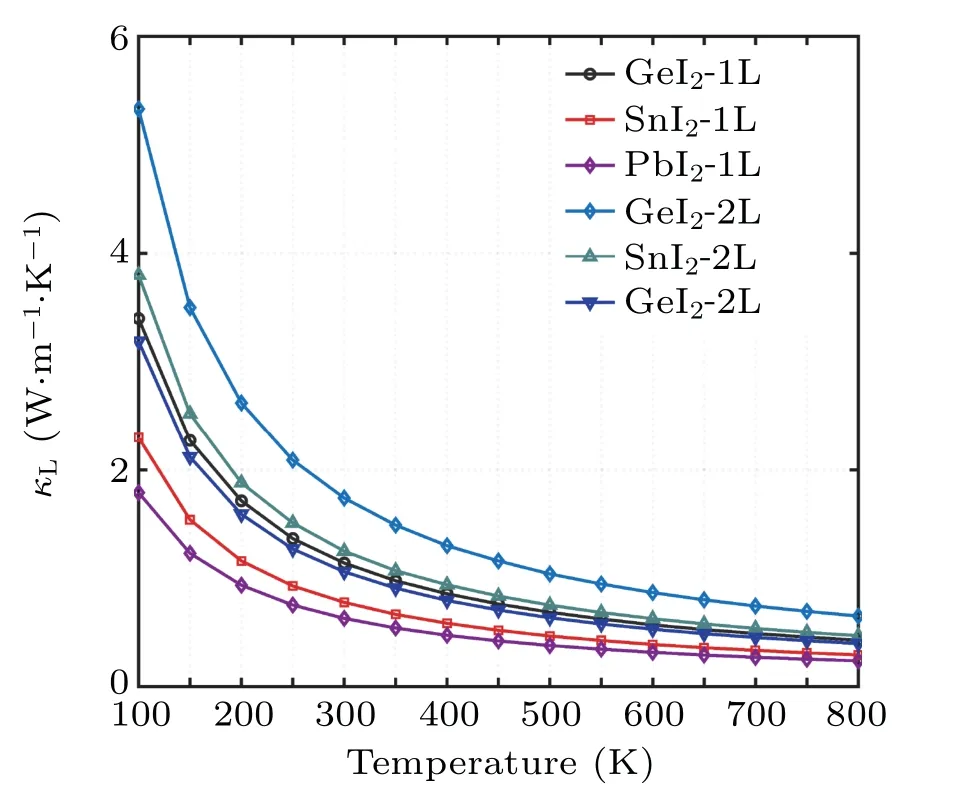
Fig.3. Lattice thermal conductivity(κL)for XI2(X=Ge,Sn,Pb)monolayers and bilayers as a function of temperature (T) calculated using iterative solutions of the phonon Boltzmann transport equation.

Fig.4. Frequency-dependent phonon group velocity(Vg)(upper panel)and phonon lifetime(τph)at 300 K(lower panel)for monolayers(black dots)and bilayers(red dots)of[(a),(d)]GeI2,[(b),(e)]SnI2,and[(c),(f)]PbI2.
Phonon lifetimeτphis an important parameter to describe phonon anharmonicity according to Eqs. (2) and (3). It can be calculated by the reciprocal of anharmonic three-phonon scattering rates(ASRs)[47,48]
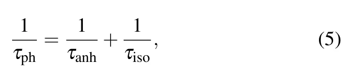
whereτph-1,τanh-1, andτiso-1represent the total scattering rate (the inversion of total lifetime of phonons), the anharmonic scattering rate,and the isotopic scattering rate,respectively. Since theτisois only related to the mass of element and has little effect on the scattering rate,[49]the value ofτphmainly depends on the anharmonic scattering rate. Our results ofτphforXI2monolayers and bilayers at 300 K are plotted in Figs.4(d)-4(f). We find that for the low frequency modes,the phonon lifetimes are longer in the bilayers(red dots)than that in the monolayers(black dots), which may explain the largerκLof bilayerXI2,as shown in Fig.3.
Next,electronic structures forXI2monolayers and bilayers have been calculated. Our DFT-PBE results show that all the calculated structures are semiconductors and the monolayer band gaps are 2.09 eV, 2.03 eV, and 2.51 eV for GeI2,SnI2,and PbI2,respectively,which are consistent with the previously reported values.[38]Given the heavy atomic mass of Sn,Pb,and I,we have taken the spin-orbital coupling(SOC)effect into consideration and present the DFT+SOC results of the band structures and DOS in Fig.5.All the calculated structures have an indirect band gap with the value a little smaller than 2 eV.The band gap values of PbI2are smaller than the experimental results for the crystalline PbI2(2.346 eV at 300 K to 2.487 eV at 20 K)[43]due to the well-known underestimation for semiconducting band gaps of the PBE functional. We thus checked the band gap values at the HSE06+SOC level of PbI2. The obtained value of band gap for PbI2monolayer,bilayer,and bulk is 2.57 eV,2.55 eV,and 2.49 eV,respectively.We find that the band gap for PbI2is not quite sensitive to the number of the layers and the value for the bulk is in good agreement with the experimental results at low temperature.The band gaps of the bilayers are slightly smaller than that of the monolayers in value,as the detailed values shown in Fig.5.We find that for all the structures at the conduction band minimum (CBM) there is a fairly strong dispersion, which hints a high electron mobility, and consequently a high electrical conductivity when carrier concentration is large enough. We also note that for all the structures there are two energy peaks located betweenΓ-MandK-Γin the valence band, whose energy differences are less than 0.1 eV.Such multiple degenerate valleys(separate pockets of Fermi surface with the same energy) at the valence band maximum (VBM) will help producing large Seebeck coefficient without causing the reduction of carrier mobility, which is beneficial to TE materials.[50-52]Considering values close to 2 eV of the band gaps,the optimal working temperature is around 2000 K according to the socalled“Eg~10kBTopt”law,[53]but we here focus on the room temperature region.
To obtain the electron transport properties ofXI2,we calculated the carrier mobility ofXI2by the deformation potential theory[54-57]

In Table 1 we list the calculated values ofE1,C2D,m∗,µ,andτat 300 K.We find a nearly isotropic behaviour in the electron mobility and relaxation time for bothXI2monolayers and bilayers. In addition, the values ofµandτfor electrons in the bilayers are much larger than that in the monolayers,which indicates a dramatic enhancement of electron transport in the bilayers. In contrast, theµandτof the holes exhibit strong anisotropy in the monolayers but are much weaker in the bilayers. When compared with the monolayers, theτfor the holes in the bilayers are larger in the armchair direction but smaller in the zigzag direction.
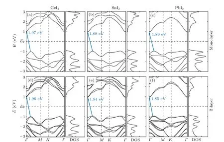
Fig.5. Electronic band structure and density of states(DOS)for monolayers(upper panel)and bilayers(lower panel)of[(a),(c)]GeI2,[(b),(e)]SnI2,and[(c),(f)]PbI2. The indirect band gaps are indicated by the blue arrows and the PBE+SOC values of band gaps are given.
To further investigate the TE performance,in Fig.6 we have plotted theS,σ,PF,andZTas a function of carrier concentrations(n)(n-type for electrons and p-type for holes)forXI2monolayers and bilayers in both armchair and zigzag directions at 300 K. As shown in Figs. 6(a)-6(f), theShas negative values for n-type doping and positive values for p-type doping. For all the calculated structures,we find that theSdisplays no directional dependency and decreases with the increasingn. The p-typeSis larger than n-type due to the degenerate valleys at the VBM. The values ofSfor the bilayers are larger than that of the monolayers.
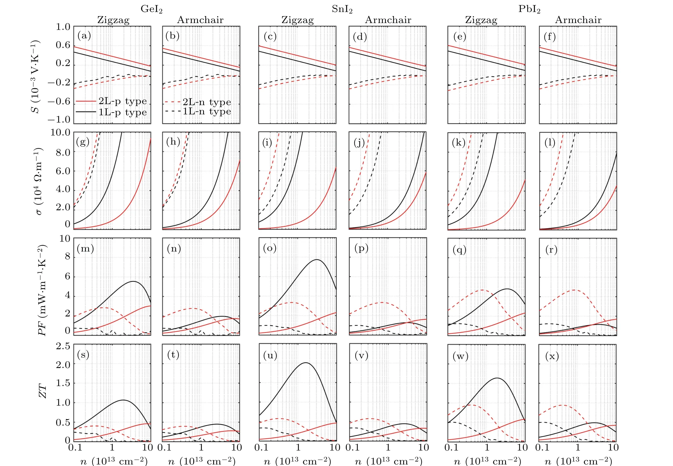
Fig.6. Calculated[(a)-(f)]Seebeck coefficients(S),[(g)-(l)]electrical conductivity(σ),[(m)-(r)]power factor(PF),[(s)-(x)]figures of merit(ZT)as a function of the carrier concentration(n)for monolayers and bilayers of GeI2 (left panel), SnI2 (middle panel), and PbI2 (right panel)at 300 K.The results along both zigzag(left sub-panel)and armchair(right sub-panel)directions are plotted. The p-type and n-type values are distinguished by solid and dashed lines. The results for monolayer and bilayer are distinguished by color.
From theσplots depicted in Figs. 6(g)-6(l), we find that the n-type conductivity keeps isotropic and is greatly larger than the p-type conductivity. The p-type conductivity of monolayers shows significant anisotropy, while for the bilayers the anisotropy is much weaker.What is more,the n-type conductivity ofXI2bilayers is larger than that of monolayers and for the p-type conductivity it is contrary. These results are consistent with the data of carrier mobility and relaxation time listed in Table 1.
The different behaviours of n-and p-type carriers mainly originate from the dramatic differences between the effective mass at the VBM of the monolayers and bilayers. As shown in Table 1,the values ofm∗for the electrons in the bilayers are close to that in the monolayers. Theµandτfor the electrons in the bilayers are about twice as large as that in the monolayers due to their largerC2D. However, the values ofm∗for the holes are generally much larger in the bilayers,leading to the significantly lowerµandτfor the holes in the bilayers compared with the monolayers.
Incorporating all the physical quantities mentioned above,in the bottom two rows of Fig.6 we have plotted thePFandZTas a function ofn. We find that the curves ofPFandZThave similar profiles. For the monolayers, bothPFandZThave much larger values for p-type doping than that for n-type doping. The maximum p-typeZTvalues reach 1.01(n= 2.10×1013cm-2), 2.01 (n= 1.69×1013cm-2), and 1.64(n=1.97×1013cm-2)at 300 K along zigzag direction in GeI2, SnI2, and PbI2monolayers, respectively. The values ofPFandZTfor p-type carriers in the bilayers(red lines)are lower than that in the monolayers(black lines). However,the n-typePFandZTare greatly enhanced in the bilayers compared to the monolayers due to the larger Seebeck coefficient and electrical conductivity.The maximum n-typeZTvalues at 300 K for GeI2,SnI2,and PbI2bilayers reach respectively 0.40(n=3.78×1012cm-2),0.58(n=3.32×1012cm-2),and 0.95(n=4.23×1012cm-2). In addition, thePFandZTfor the bilayers display much weaker in-plane anisotropy compared with the monolayers. The nearly isotropicZTvalues provide consistent in-plane TE performance independent of direction forXI2bilayers.
4. Conclusion
In summary, by combiningab initioDFT calculations with the Boltzmann transport theory,we investigated the electrical and thermal transport properties and the TE performance of theXI2(X=Ge,Sn,Pb)monolayers and bilayers. Phonon spectra was calculated and the essentially absence of imaginary frequencies confirms the dynamical stability of all the 2DXI2structures. The relatively low frequency of the optical modes leads to their as significant contribution to the thermal conductivity as the acoustic modes,which is confirmed by the group velocity distribution. The values of the lattice thermal conductivityκLat 300 K for the bilayers are 1.74 W·m-1·K-1,1.25 W·m-1·K-1, and 1.05 W·m-1·K-1for GeI2, SnI2, and PbI2, respectively, which are about 1.6 times as large as that for the corresponding monolayers but still at a relatively low level.Electronic structure calculations show that all the monolayer and bilayer structures are semiconducting with an indirect band gap close to 2 eV and the bilayers have slightly smaller values of band gaps than the monolayers. In addition,theXI2bilayers have much higher electron mobility and relaxation time than the corresponding monolayers. The TE performance calculations show that the monolayers exhibit dramatically anisotropic TE performance and have higher efficiency for p-type doping than the bilayers.The highest p-typeZTvalues along zigzag direction reach 1.01,2.01,and 1.64 at 300 K for GeI2, SnI2, and PbI2monolayers, respectively. The bilayers,however,exhibit nearly isotropic TE performance and have higher efficiency for n-type doping than the monolayers. The highest n-typeZTvalues reach 0.40, 0.58, and 0.95 at 300 K for GeI2, SnI2, and PbI2bilayers, respectively. The nearly isotropicZTvalues provide consistent in-plane TE performance independent of direction forXI2bilayers.
Although the experimental results for the TE performance have not been reported so far,low thermal conductivity of PbI2has been experimentally measured[43]and 2D SnI2down to the monolayer has also been successfully prepared in experiment recently.[60]These encouraging experimental progresses supply a reasonable prospect of the applications for 2DXI2in TE materials.Our finding of the difference between the monolayer and bilayer for the doping type with superior figure of merit and the in-plane anisotropy indicates that the inter-layer interaction plays an important role in the TE performance ofXI2. It provides an effective tunability on the TE characteristics of few-layerXI2and will be of significant value in the relative experimental study in the future.
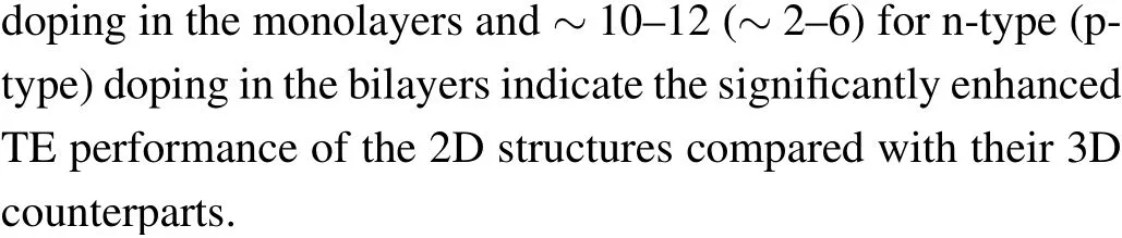
Appendix A:The confinement effect
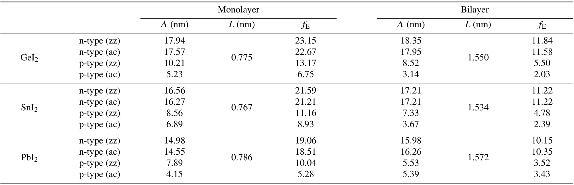
Table A1. The PF enhancement factor(fE)for XI2 (X =Ge,Sn,Pb)monolayers and bilayers. L is the spatial confinement length and Λ is the thermal de Broglie wavelength. Calculated values in zigzag and armchair directions are denoted by‘zz’and‘ac’.
Acknowledgements
Project supported by the Fundamental Research Fund for the Central Universities and the Zhongying Young Scholar Program of Southeast University. We thank the Big Data Computing Center of Southeast University for providing facility support for performing calculations presented in this manuscript.
- Chinese Physics B的其它文章
- Quantum walk search algorithm for multi-objective searching with iteration auto-controlling on hypercube
- Protecting geometric quantum discord via partially collapsing measurements of two qubits in multiple bosonic reservoirs
- Manipulating vortices in F =2 Bose-Einstein condensates through magnetic field and spin-orbit coupling
- Beating standard quantum limit via two-axis magnetic susceptibility measurement
- Neural-mechanism-driven image block encryption algorithm incorporating a hyperchaotic system and cloud model
- Anti-function solution of uniaxial anisotropic Stoner-Wohlfarth model