
Lateral β-Ga2O3 Schottky barrier diode fabricated on(-201)single crystal substrate and its temperature-dependent current-voltage characteristics
2022-04-12 03:44PeiPeiMa马培培JunZheng郑军YaBaoZhang张亚宝XiangQuanLiu刘香全ZhiLiu刘智YuHuaZuo左玉华ChunLaiXue薛春来andBuWenCheng成步文
Chinese Physics B 2022年4期
Pei-Pei Ma(马培培) Jun Zheng(郑军) Ya-Bao Zhang(张亚宝) Xiang-Quan Liu(刘香全)Zhi Liu(刘智) Yu-Hua Zuo(左玉华) Chun-Lai Xue(薛春来) and Bu-Wen Cheng(成步文)
1State Key Laboratory on Integrated Optoelectronics,Institute of Semiconductors,Chinese Academy of Sciences,Beijing 100083,China
2Center of Materials Science and Optoelectronics Engineering,University of Chinese Academy of Sciences,Beijing 100049,China
Keywords: β-Ga2O3,Schottky barrier diodes,rectifying ability,breakdown voltage
1. Introduction
Recently, gallium oxide (Ga2O3) has received much attention because of its unique properties,[1-3]including a wide bandgap(4.5 eV-4.8 eV)and a high breakdown electric field of 8 MV/cm. The Baliga’s figure of merit ofβ-Ga2O3reaches up to 3444, which is significantly higher than that of silicon carbide (SiC) and gallium nitride (GaN).[4-6]Moreover,high-quality large-size single-crystalβ-Ga2O3substrates can be easily grown by low-cost and stable melting methods.[7-10]Thus,β-Ga2O3materials have great potential applications in power devices. In power electronic circuits, two types of power devices each play a key role in power conversion.The first type is the switching transistor, which controls the switching state of the current transmission to regulate the total power, and the second type is the rectifier diode, which controls the transmission direction of the current. As the Ptype doping technology ofβ-Ga2O3materials is very difficult,β-Ga2O3wafers are all of n-type semiconductor and more applicable for unipolar power devices, such as metal-oxidesemiconductor field-effect transistors(MOSFETs)and Schottky barrier diodes (SBDs).[11,12]Considerable efforts have been made to enhance the performances ofβ-Ga2O3power devices, and remarkable results have been achieved. For example, field-plated MOSFETs each with a high breakdown voltage(BV)[13]and high power figure of merit(P-FOM)[14]have been reported.
The SBDs are important for power rectification applications due to their advantages of low turn-on voltage, fast switching speed, and low switching loss.[15,16]Theβ-Ga2O3SBDs reported possess almost vertical structures by homoepitaxy of high-qualityβ-Ga2O3drift layers.[17-21]For example,Allenet al.reported that vertical structured SBD with a breakdown electric field of up to 3.5 MV/cm involves an edge termination and a small-angle beveled field plate.[22]Liet al.reported vertical trench SBD with a BV of 2.89 kV and PFOM of 0.95 GW/cm2.[23]Unlike vertical SBD structure,the lateral SBD structure can be fabricated on single-crystalβ-Ga2O3substrate with the highest quality drift layer, while avoiding the difficult and costly hydride vapor phase epitaxy homoepitaxial growth techniques. However, the current flowing in a lateral structure device is limited in the extremely thin channel layer; therefore, there are few reports on lateralβ-Ga2O3SBDs.[24-26]For example, lateral SBD with the highest forward current density of 40 mA/mm has been fabricated by transferringβ-Ga2O3nano-membranes.
In this study, we fabricate lateral SBDs on high-quality single-crystalβ-Ga2O3substrates by designing L-shaped electrodes. By introducing the sidewall electrodes on both sides of the conductive channel,the high forward current density of 223 mA/mm and the low specific on resistance(Ron,sp)of 4.7 mΩ·cm2are achieved. In addition, the device shows a high reverse voltage and good rectifying ability. These results indicate that lateralβ-Ga2O3SBDs have great potential applications in power electronics.
2. Experimental details
The unintentionally doped (UID) (-201) n-typeβ-Ga2O3bulk crystal with carrier concentration about was 2.2×1017cm-3used in this work for fabricating lateral SBD. Figure 1(a) shows the high resolution x-ray diffraction(HRXRD)2θ-ωscans of theβ-Ga2O3substrate to characterize the crystal quality. A schematic of the device is shown in Fig. 1(b). The conductive channels of carriers were designed along the[010]direction,which has high carrier mobility. Moreover,it was found that the dry etch has low damage to the(010)sidewalls,providing the high performance of lateral SBD.The lateralβ-Ga2O3SBD structure was fabricated by depositing a 300-nm-thick passivation layer on the top of the substrate by plasma-enhanced chemical vapor deposition(PECVD).The cathode and anode regions were shaped by dry etching,[27]respectively. The Si implantation and annealing treatment were performed in the cathode region of the sidewall and bottom mesa to form an ohmic contact.[28]The doping concentration is estimated at~5×1019cm-3, based on the simulation. After Si activation,the Ti/Au electrodes were evaporated and implemented rapid thermal annealing(RTA)at 475°C for 1 min.Based on the transfer length method(TLM),the sheet resistance (RSH) and contact resistance (RC) were extracted to be 176 Ω and 1 Ω·mm, respectively. Finally, a Schottky contact was introduced by stacking metals of Ni/Au,followed by the steps of device passivation,pads opening and metal thickening. An optical micrograph of the fabricated device is shown in Fig. 1(c). The current-voltage characterizations were tested in the dark by using an Agilent B1500A semiconductor parameter analyzer. The reverse breakdown characterizations were performed by using a Keithley 4200-SCS.
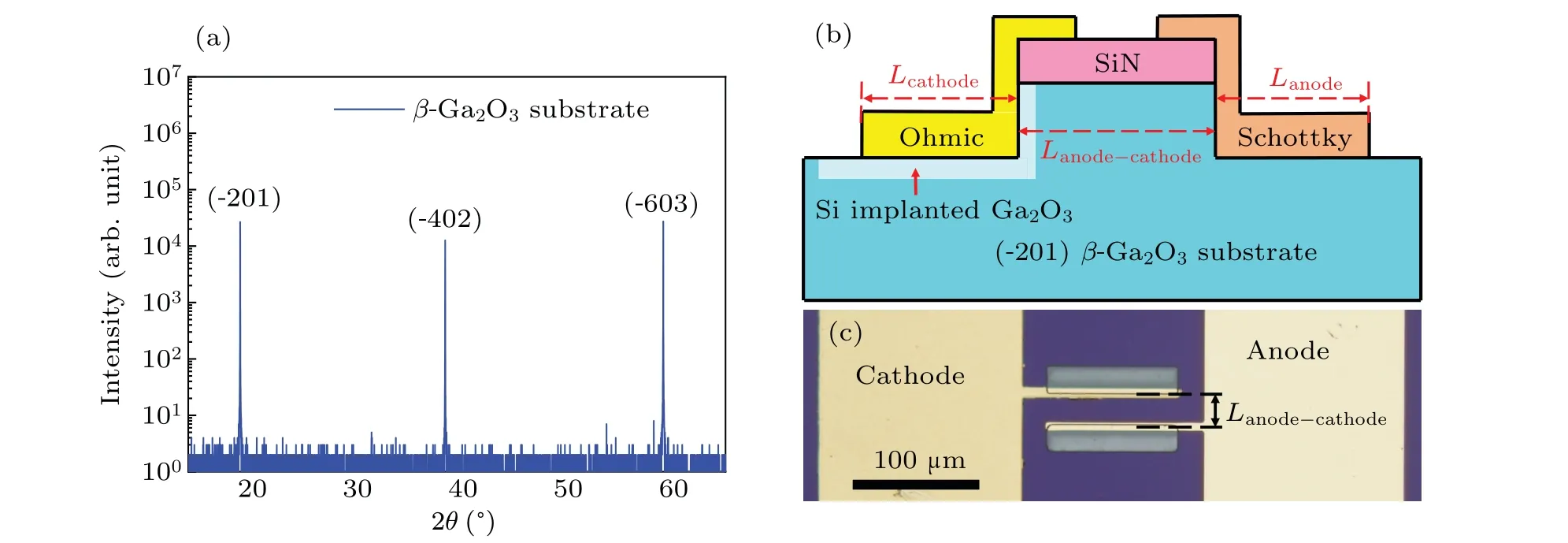
Fig. 1. (a) HRXRD curve of (-201) β-Ga2O3 single crystal substrate, (b) schematic diagram of device cross-section, and (c) optical micrograph of a fabricated SBD.
3. Results and discussion
Figure 2(a)shows the forwardJ-Von a linear scale and differential resistance-voltage (Diff.Ron-V) characteristics for lateral SBDs with different values ofLAC. From the DC measurements, a current density of 223 mA/mm, which is one order of magnitude higher than the current density of the reported lateralβ-Ga2O3SBDs,[24,25]and a very lowVonis achieved to be 0.98 V.The anode length(LA)and the cathode length (LC) are 5 µm. The value of Diff.Ronis extracted to be 13.5 Ω·mm,yielding the value ofRon,spof 4.7 mΩ·cm2forLAC=25µm by considering thatRon,sp=Ron×(LA+LAC+LC). Figure 2(b) shows the forward current density-voltage(J-V)characteristics of the lateral SBD withLAC=25µm on a semi-logarithmic scale.TheIon/Ioffratio is as high as 109.A subthreshold swing of 67 mV/dec is extracted from the current density between 10-6mA/mm and 10-3mA/mm. Figure 2(c)demonstrates that the measured current is nearly proportional to the device width.
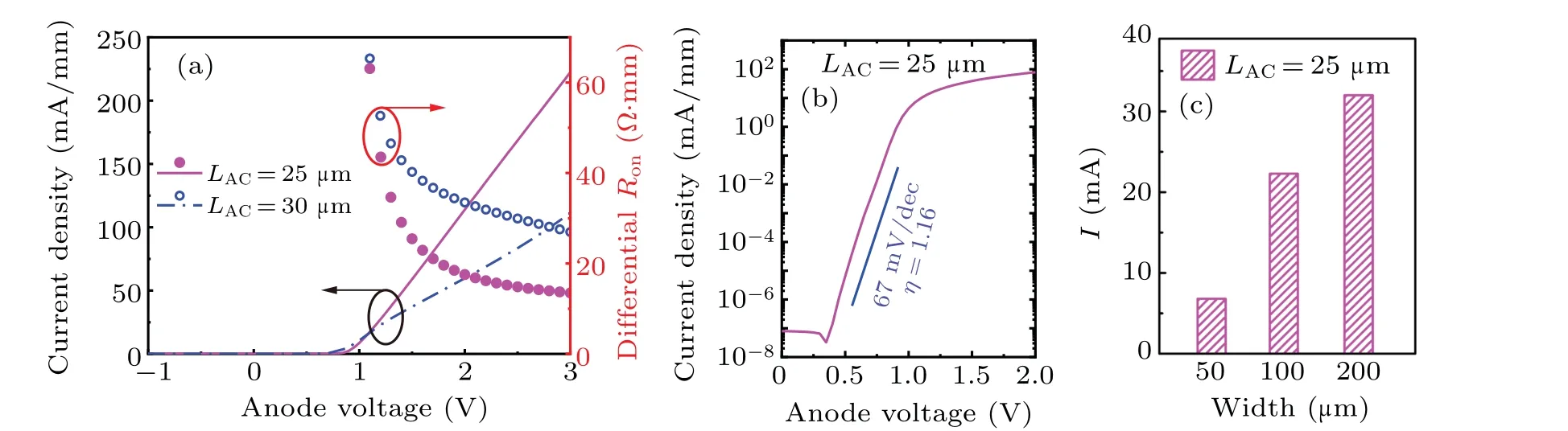
Fig. 2. (a) Linear-scale plots of forward J-V and Diff. Ron-V characteristics, (b) log-scale forward J-V characteristics of the fabricated lateral SBD with LAC=25µm,and(c)dependence of current on the width of SBD for LAC=25µm.
Figure 3 shows the reverseI-Vcharacteristic of theβ-Ga2O3SBD. The device can withstand a reverse voltage as high as 200 V without breakdown, much higher than otherβ-Ga2O3SBDs using single crystals[29]and lateral GaN SBDs.[15]We cannot further increase the voltage for testing due to the limitation of the test instrument. Moreover, the breakdown voltage will be larger than 200 V, for the reverse current value is about 10-7A under the maximum test voltage.

Fig.3. Reverse I-V characteristic of Ni/β-Ga2O3 SBD with LAC=30µm.

According to the thermionic emission (TE) model, the forwardJ-Vrelationship can be expressed by the equation of usingm∗= 0.23m0~ 0.34m0calculated from firstprinciples;[17,30]qΦb,0is the height of Schottky barrier at zero bias and given byqΦb,0=qVbi+(Ec-Ef)-qΦifbl,withqVbi,Ec,Ef,andqΔΦifblbeing the zero bias built-in potential,minimum value of conduction band,Fermi level,and potential barrier reduction caused by image force.
The forward temperature-dependentJ-Vcharacteristics of theβ-Ga2O3SBD in a semi-logarithmic scale are measured as shown in Fig. 4(a). By increasing the working temperature from 20°C to 150°C in steps of 25°C, these characteristics evolve smoothly. Analysis of the linear region of the logJ-Vplot shows thatJ0andηcan be calculated from the slope and intercept. Figure 4(b) is Richardson’s plot, that is,the [ln(J0/T2)-1/kT] plot. By fitting the test data linearly,qΦb,0andA∗are obtained from slope and intercept, respectively,to beqΦb,0=1.3 eV andA∗=29.7 A/cm2·K2. The extractedqΦb,0values is higher than those of Ni/Ga2O3[19,20,24]and TiN/Ga2O3Schottky contact,[26]and even higher than that of Pt/Ga2O3contact.[17]The highqΦb,0is mainly caused by the low doping concentration of the UID wafer.[23,31]Moreover, theA∗value is smaller than other reported experimental results[17,18]but matches well with previous first-principles calculation results. The lowerA∗may be due to the low effective density of states in the conduction band[32]or the uneven distribution of Schottky barrier.[33]Figure 4(c) also displays the plots of the temperature dependence ofqΦb,0andηderived by fitting theJ-Vcurves,showing they slightly decrease to about 1.30±0.05 eV and 1.16±0.05 eV as the temperature increases from 20°C to 150°C. Both theqΦb,0values obtained from the Richardson’s plot and fittedJ-Vcurves are in accordance with each other. The reason for a weak temperature dependence ofqΦb,0is thatEc-Efhas a positive temperature coefficient whileqVbiis negatively correlated with temperature. As the temperature increases, more electrons have enough energy to cross the barrier,resulting in slight decrease ofqΦb,0andη.[17]
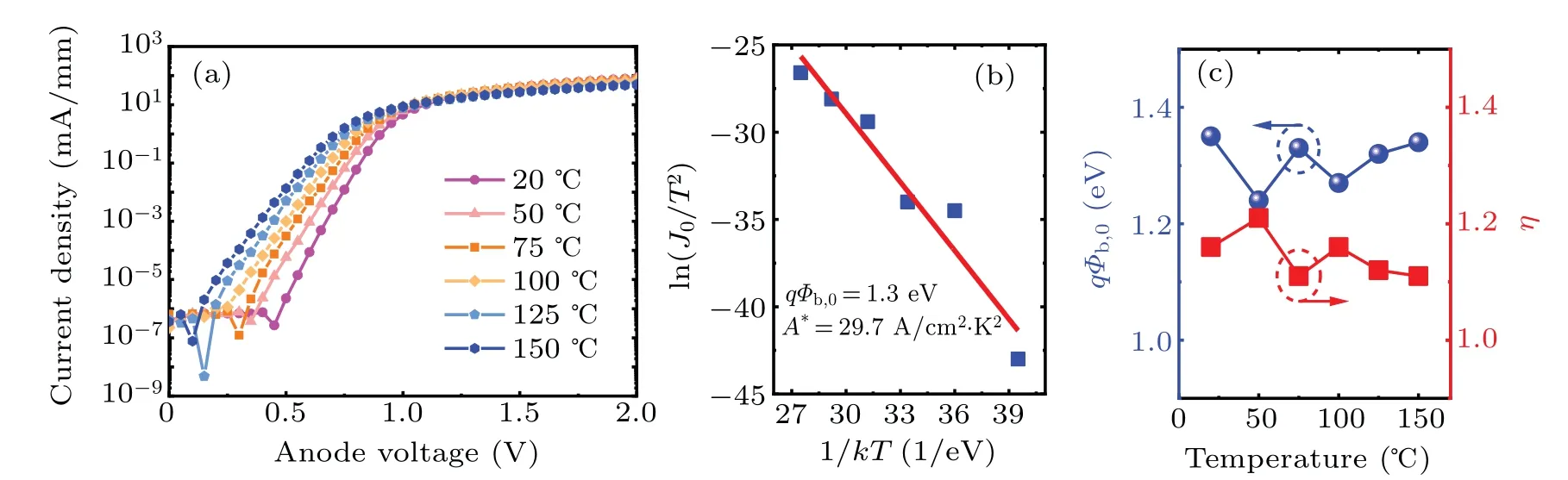
Fig.4. (a)Forward J-V-T characteristics on a log scale of lateral SBD with LAC =25µm in a temperature range of 20 °C-150 °C,(b)Richardson’s plot of lateral SBD with LAC=25µm,and(c)temperature dependence of extracted qΦb,0 and η.
The benchmark performances of some state-of-the-art representativeβ-Ga2O3SBDs with marked vertical and lateral structures,are shown in Table 1. It is evident that the SBD in this work shows the highest forward current density among all the lateralβ-Ga2O3SBDs reported so far. Moreover, in this work, the SBD presents an extremely lowRon,spbecause it is fabricated on a high-quality single substrate with low dislocation.[34]By thickening theβ-Ga2O3etching depth to enlarge the metal contact profile,the forward current density can be further enhanced as theRon,spwill be reduced,[16]whereas theRon,spof vertical SBD can only be reduced by increasing the carrier concentration at the cost of reduced BV.
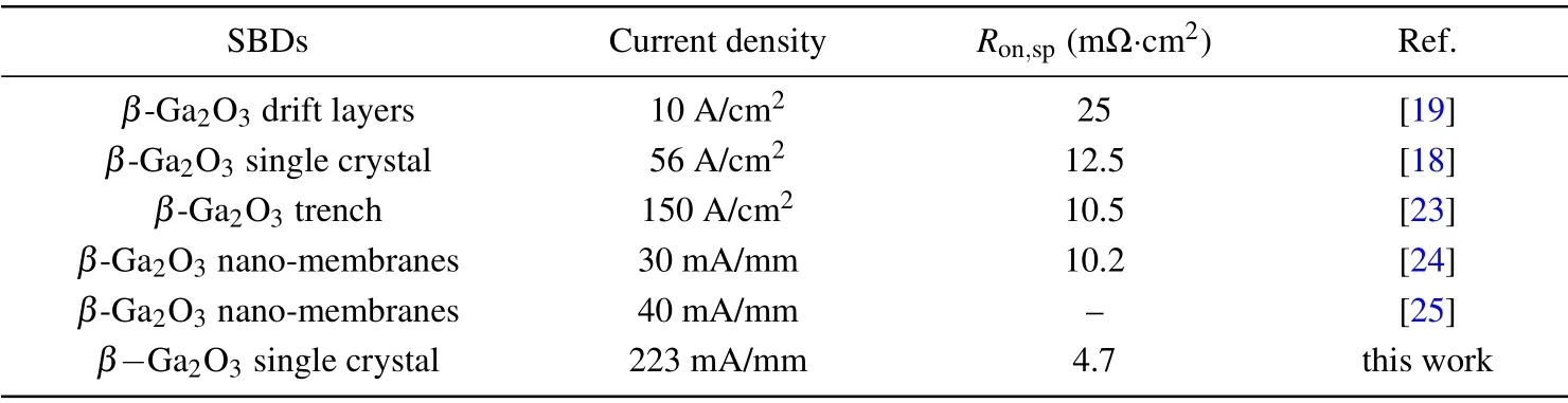
Table 1. Comparison among characteristic parameters of β-Ga2O3 SBDs.
4. Conclusions
In this work,the lateralβ-Ga2O3SBDs each with an innovative structure adopting an unintentionally doped (-201)β-Ga2O3single crystal have been demonstrated. The fabricated devices each with a simple L-shaped electrode structure exhibit outstanding forward current density and lowRon,spwith respect to other lateral SBDs. The lateral SBD fabricated onβ-Ga2O3single crystal substrate has a high-quality drift channel in comparison with those fabricated by homoepitaxial techniques. The lateral SBDs in this work have broad applications, and may serve as an promising candidate for future high-power electronic devices.
Acknowledgements
Project supported by the National Key Research and Development Program of China(Grant No.2018YFB2200500),the National Natural Science Foundation of China (Grant Nos. 62050073, 62090054, and 61975196), and the Key Research Program of Frontier Sciences, Chinese Academy of Sciences(Grant No.QYZDY-SSW-JSC022).
- Chinese Physics B的其它文章
- Quantum walk search algorithm for multi-objective searching with iteration auto-controlling on hypercube
- Protecting geometric quantum discord via partially collapsing measurements of two qubits in multiple bosonic reservoirs
- Manipulating vortices in F =2 Bose-Einstein condensates through magnetic field and spin-orbit coupling
- Beating standard quantum limit via two-axis magnetic susceptibility measurement
- Neural-mechanism-driven image block encryption algorithm incorporating a hyperchaotic system and cloud model
- Anti-function solution of uniaxial anisotropic Stoner-Wohlfarth model