
Fast-switching SOI-LIGBT with compound dielectric buried layer and assistant-depletion trench
2022-04-12 03:44ChunzaoWang王春早BaoxingDuan段宝兴LichengSun孙李诚andYintangYang杨银堂
Chinese Physics B 2022年4期
Chunzao Wang(王春早) Baoxing Duan(段宝兴) Licheng Sun(孙李诚) and Yintang Yang(杨银堂)
1Key Laboratory of the Ministry of Education for Wide Band-Gap Semiconductor Materials and Devices,School of Microelectronics,Xidian University,Xi’an 710071,China
2Department of Physics and Electronic Information,Shaoxing University,Shaoxing 312000,China
Keywords: lateral insulated gate bipolar transistor,breakdown voltage,electric field modulation,turn-off loss
1. Introduction
Because of the lower turn-on voltage,better thermal stability and easier integration,[1-3]silicon-on-insulator lateralinsulated gate bipolar transistors (SOI-LIGBTs) are common devices in power integrated circuits that are prevalent for example in automotive electronics and switching mode power supplies. The low forward voltage drop (VF) arises a modulation in conductivity in the drift region during turn-on. Concurrently, many injected nonequilibrium carriers need to be extracted or recombined during turn-off. The shortcoming is that it leads to a large turn-off loss(EOFF).[4-6]
One important challenge for power semiconductor devices of the LIGBT is to obtain an optimal compromise betweenVFandEOFF. The main ways of generating a betterVFEOFFtrade-off are through: i) anode engineering including a shorted anode structure,a Schottky anode structure and a segmented NPN anode structure,which are realized by adding an extra carrier extraction channel;[7-10]ii)effectively accelerating carrier recombination by shortening carrier lifetime with high-power irradiations of protons and electrons,[11,12]and iii)creating deep oxide trenches that assist in sustaining the lateral field from the anode side,so as to increase the breakdown voltage (BV) and shorten the length of the drift region while maintaining a superiorVF-EOFFtrade-off.[13-15]Moreover,to optimize the distribution of surface electric field, an electric field modulation is introduced by adjusting the size and composition of the buried layer,[16,17]thereby improving BV and reducing the device pitch.
In this paper, a fast-switching SOI-LIGBT with compound dielectric buried layer (CDBL) and assistant depletion trench(ADT)is investigated and simulated. New electric field peaks are generated with the presence of the CDBL, resulting in a uniform distribution of the surface electric field and a shorter drift region length that improves the breakdown characteristics and reduces the total number of carriers stored in the drift region. Moreover, the stored carriers are extracted rapidly through an expedited depletion of the N-drift region by the ADT.Consequently,the proposed device exhibits a lower turn-off loss than a conventional SOI LIGBT.This study was performed by using Sentaurus device simulation tools,which contain models of the Enormal mobility, Auger recombination, high-field-saturation mobility, Philips unified mobility,Lackner avalanche generation, and the theory of Shockley-Read-Hall recombination.
2. Device structure and description
The SOI LIGBT (Fig. 1) comprises an oxide segment and a low-kdielectric segment that are alternately placed as a buried layer and both have the same thicknesses(Tox).The relative permittivitykIof the low-kdielectric layer increases from 1 to 3 with a step size of 0.5,and akIvalue near 1 is obtained by employing buried gaps of air or gas. The dielectric layer introduced into the buried air gap structure is formed by removing a SiGe layer using isotropic plasma dry etching.[18]In addition,a gas-dielectric process to achieve a minimum physically possible value for the dielectric constant was instigated in which the carbon trench in the buried layer reacts with oxygen in an oxidation furnace to form carbon dioxide gas.[19]WithNbeing the number of alternately placed oxide and low-kdielectric segments, we setNdandTdas the concentration and thickness of the N-drift region,respectively. When the lateral length of the device is much larger than the vertical thickness of the top Si layer, breakdown occurs along the vertical direction. New electric field peaks are produced because of the variable-kburied layer, which raises the electric field at the surface of the substrate of differentkIand introduces electric field peaks on both sides of the p-n junction and the n-n+junction. This rise helps to produce a uniform surface electric field distribution and thus increase the BV.
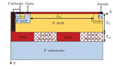
Fig.1. Schematic cross-section of the proposed CDBL SOI LIGBT.
From another perspective, while maintaining the same BV value,both the length of the proposed device and the total number of stored carriers in the drift region decrease significantly. Hence, a superiorVF-EOFFtrade-off is obtained. The ADT consisting of an enclosed oxide and grounded polysilicon is located leftmost of the cathode and connected to the P+cathode. The ADT reshapes laterally the electric potential distribution,which expedites the depletion of the drift region and generates an additional heat flow with the formation of a hole inversion layer along the ADT.
3. Results and discussion
Table 1 provides a list of the main simulation parameter settings for both the proposed structure and the conventional structure. The concentrations of the drift region for all devices are optimized to meet the reduced surface field (RESURF)condition. Because the dielectric at the interface between the top Si layer and the buried layer changes (Fig. 2), two new surface electric field peaks in the proposed device appear near M and N through the coupling of the electric field peaks for the new interface. Moreover, the new electric field peaks reduce the original electric field peak at the gate and drain edges,ensuring a more uniform electric field distribution within the proposed CDBL LIGBT structure. Furthermore, the lowerkIis, the higher the electric field peak is. When the minimum value ofkIis 1,the internal electric field peak reaches its maximum value,thereby improving the BV of the proposed CDBL LIGBT correspondingly.
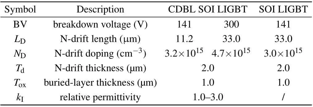
Table 1. Design parameters of the two devices.
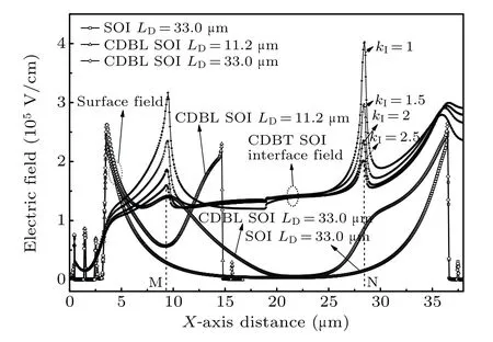
Fig. 2. Electric field distributions on the bottom interface of the Si/buried layer and the surface.
The simulation results of the surface electric potential distributions of a conventional SOI LIGBT(LD=33µm,kI=1,N=4 andTox=1µm)and the proposed CDBL SOI LIGBT(LD=33µm andTox=1µm)at breakdown[Fig.3(a)]show that their BVs are approximately 300 V and 141 V, respectively,despite the device size being the same. This shows that for the sameLDthe BV of the proposed CDBL SOI LIGBT is 113% higher compared with the conventional SOI LIGBT.Furthermore, when maintaining the same BV of 141 V, the length of the drift region of the CDBL SOI LIGBT is 11.2µm,which is approximate a third of the length (33 µm) of a conventional structure. Consequently,the CDBL of the proposed LIGBT creates a drift region of shorter length and a higher BV by modulating the electric field. The equipotential contour of the proposed CDBL LIGBT and the conventional SOI LIGBT at breakdown[Fig.3(b)]manifest a laterally reshaped electric potential distribution in the structure because of the ADT, which expedites the depletion of the drift region and contributes to a fast extraction of the stored carriers in the offstate.
Fig.3. (a)Horizontal surface electric potential distributions and(b)equipotential contour distributions of the proposed CDBL LIGBT and the conventional SOI LIGBT at breakdown.
The dependence of the BV onToxfor variouskI[Fig.4(a)]exhibits linearity withToxand an inverse proportionality withkI. To better analyze this relationship,breakdown characteristics were investigated by using an analytical model taking into account the effects of electric field modulation. With a reverse bias applied to the device,the completely depleted drift region is divided up within the variable-kIburied layer. The potential distribution functionφi(x,y) in each drift region satisfies the two-dimensional Poisson equation[20,21]
Through applying a second-order Taylor series expansion,the potential distributionφi(x,y)of the drift region in theydirection is expressed as

After a series of derivations and calculations, the surface potential at the interface of regionsiandi+1 of the device is
where
Clearly, from Eqs. (4)-(6), the characteristic thicknesstiincreases with increasingToxand decreases with increasingkI.Accordingly, the BV also increases, which is consistent with the simulation results[Fig.4(a)]. The drift region of the proposed CDBL SOI LIGBT is divided intoNequal parts according to the differentkIof the buried layer. The maximum BV is 316 V whenkIis 1 andNis 2. Moreover,with increasingkI,the BV has little effect on valueN[see Fig.4(b)].
The forward characteristics[Fig.5(a)]of the conventional SOI LIGBT and the proposed CDBL SOI LIGBT with the same BV (141 V) show that, because of its shorterLDof 11.2 µm, the latter acquires a lowerVFof 1.02 V atJC=100 A/cm2that is significantly less thanVFof 1.64 V for the conventional structure. The proposed device has a better current capability. The dependence ofVFonToxfor differentkI[Fig. 5(b)] exhibits a linear relationship, and lowerVFvalues are obtained because of the optimal drift concentration. However,the functional relationship betweenVFandkIis weak and demonstrates that changes inkIinfluence the forward conduction characteristics less,andVFonly changes by approximately 0.02 V betweenkIfrom 3 to 1.
From the turn-off equivalent circuit[Fig.6(a),inset],the inductive turn-off characteristics for the proposed CDBL SOI LIGBT (LD= 11.2 µm) and the conventional SOI LIGBT(LD=33 µm) were obtained [Fig. 6(a)]. The turn-off time(Toff= 71.4 ns) for the CDBL SOI LIGBT is 48.9% lower than that of the conventional SOI LIGBT(Toff=139.6 ns). In addition, the area of the overlapped region between the current and voltage curves of the CDBL SOI LIGBT is smaller than that of the conventional SOI LIGBT during turn-off. The decrease indicates that the proposed structure gives a lowerEOFF. This is because the number of stored carriers in a drift region of shorterLDis obviously lower. In addition,the ADT contributes by laterally reshaping the electric potential distribution and expediting the depletion of drift region. Therefore,by changing the concentrations of the P+ anode, lowerEOFFandVFare obtained with the proposed CDBL SOI LIGBT[Fig. 6(b)]. By adjusting the anode concentration, theEOFFof the CDBL SOI LIGBT is 88.7%lower than that of the conventional SOI LIGBT for the sameVF.
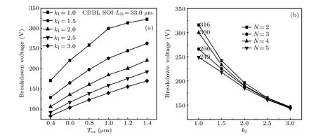
Fig.4. BV as a function of Tox and kI: (a)BV versus Tox and(b)BV versus kI.
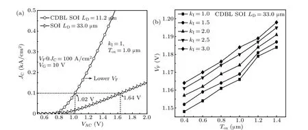
Fig.5. Forward characteristics of the conventional and proposed structure: (a)profiles of the simulated forward characteristics and(b)VF as a function of Tox for various kI.
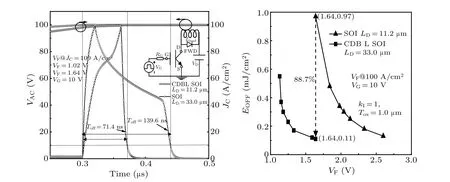
Fig.6. (a)Inductive turn-off characteristics and(b)EOFF versus VF for the CDBL and conventional SOI LIGBTs.
A failure in self-heating appears during the on-state of the device when the intrinsic temperature of the device increases rapidly. A hole inversion layer is realized along the ADT of the proposed structure,which acts as an extra heat dissipation path during a short-circuit [Fig. 7(a)]. Therefore, the proposed CDBL SOI LIGBT exhibits a lower maximum lattice temperature(681 K) in comparison with the conventional SOI LIGBT (753 K) [Fig. 7(b)]. Correspondingly, the short-circuit failure time of the proposed CDBL SOI LIGBT is 45% longer than that of the conventional SOI LIGBT (Fig. 8), which indicates a better short-circuit robustness for the proposed structure.

Fig. 7. (a) Hole heat flux distributions and (b) lattice temperature profiles for the CDBL and conventional SOI LIGBTs under short-circuit condition with VA=80 V.

Fig.8. Short-circuit waves for the CDBL SOI LIGBT and conventional SOI LIGBT.
The steps in fabrication of the proposed CDBL LIGBT are similar to those for a conventional SOI LIGBT[Fig.9(a)].One major difference between the two devices concerns the formation of the lowkdielectric. In the flow of the low-kdielectric implementation process[Fig.9(b)],[22]the trenches are firstly etched in the insulator film, which is located in the lowkdielectric regions,and subsequently,carbon is produced during either a physical or a chemical vapor deposition,which fills up the trenches with carbon. Next,an approximately 50-nm-thick thin insulator film is deposited over the lowkdielectric area. Finally, when oxygen is diffused through the thin layer of insulator,a thermal treatment of about 450°C is performed in the oxygen atmosphere of the furnace. The carbon then reacts with oxygen to form carbon dioxide that pervades the spaces,thereby forming the ultra-lowkdielectric regions.
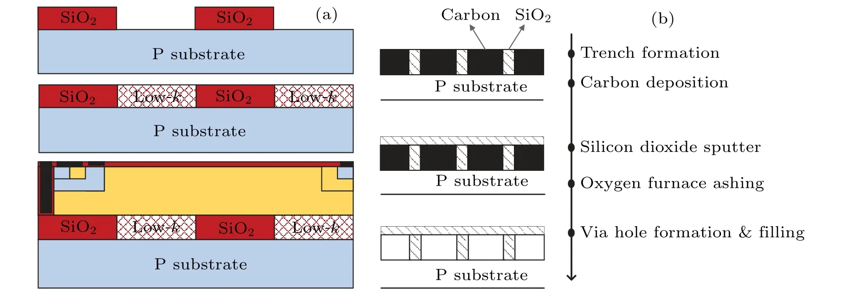
Fig.9. Key process steps of the CDBL LIGBT:(a)basic process flows,(b)low k dielectric implementation process.
4. Conclusion
A SOI LIGBT with a CDBL and an ADT was proposed and investigated. By employing a CDBL, two electric field peaks were produced to optimize the surface electric field distributions. The BV of the LIGBT was improved as a result of a more uniform electric field distribution. Simulation results of the BV for the proposed CDBL SOI LIGBT showed an increase of 113%over that for the conventional SOI LIGBT under the sameLDcondition. This increase leaded to a shorter length of the drift region and a smaller number of stored carriers, compared with the conventional SOI LIGBT. The proposed CDBL SOI LIGBT exhibited a betterVF-EOFFtradeoff. Moreover, aided by the ADT, a rapid extraction of the stored carriers and a high switching speed were achieved. We demonstrated also that self-heating within the proposed CDBL SOI LIGBT was alleviated effectively.
Acknowledgements
Project supported by the National Basic Research Program of China(Grant No.2015CB351906)and Science Foundation for Distinguished Young Scholars of Shaanxi Province,China(Grant No.2018JC-017).

- Chinese Physics B的其它文章
- Quantum walk search algorithm for multi-objective searching with iteration auto-controlling on hypercube
- Protecting geometric quantum discord via partially collapsing measurements of two qubits in multiple bosonic reservoirs
- Manipulating vortices in F =2 Bose-Einstein condensates through magnetic field and spin-orbit coupling
- Beating standard quantum limit via two-axis magnetic susceptibility measurement
- Neural-mechanism-driven image block encryption algorithm incorporating a hyperchaotic system and cloud model
- Anti-function solution of uniaxial anisotropic Stoner-Wohlfarth model