
Effect of anode area on the sensing mechanism of vertical GaN Schottky barrier diode temperature sensor
2022-04-12 03:48JiYaoDu都继瑶XiaoBoLi李小波TaoFeiPu蒲涛飞andJinPingAo敖金平
Chinese Physics B 2022年4期
关键词:金平
Ji-Yao Du(都继瑶) Xiao-Bo Li(李小波) Tao-Fei Pu(蒲涛飞) and Jin-Ping Ao(敖金平)
1School of Automation and Electrical Engineering,Shenyang Ligong University,Shenyang 110159,China
2Institute of Technology and Science,Tokushima University,Tokushima,Japan
Keywords: GaN,temperature sensor,Schottky contact,vertical diode
1. Introduction
Gallium nitride (GaN) based Schottky barrier diodes(SBDs) are key components for the next-generation high power and high switching frequency devices,which are commonly adopted in switching power supply, wireless communications, drivers, and so on.[1-4]Compared with the planar SBDs fabricated on the AlGaN/GaN structure,vertical devices can achieve high power density and high breakdown voltage by simply increasing the drift layer thickness other than extending the gate-to-drain distance.[5-10]Therefore,vertical devices are preferable to sink chip size and decrease the cost.Especially,with the tremendous progress in high quality GaN substrates, vertical GaN SBDs have attracted a great deal of attention in recent years.
On the other hand, GaN devices commonly generate heat during static on-state and on/off switching.[11]This heat dissipation will drastically increase the junction temperature especially for vertical devices which handle higher power densities. Generally,electrical parameters of SBDs are temperature-dependent and will be degraded under a relatively high temperature.[12]Hence, temperature monitoring plays a key role in ensuring safe operation or quality control. However, the accuracy and reliability of the conventional thermocouples or resistive temperature sensors do not meet the request of high temperature environment.
Alternatively,GaN based Schottky barrier diodes(SBDs)are a kind of promising candidates forin situtemperature sensor applications due to the wide bandgap, good linearity, and long-term stability. In our previous study, lateral,quasi-vertical and vertical GaN-compatible temperature sensors were fabricated and evaluated with thermally stable TiN anode.[13-16]When the SBD works in sub-threshold region,the forward voltage at a fixed relatively small current level decreases linearly versus temperature. It was demonstrated that the sensitivity of the lateral and quasi-vertical SBD is dependent on the anode area. However,the effect of anode area of a vertical diode on the sensing characteristics is not investigated extensively. In this work,vertical GaN SBDs with various anode sizes are proposed to investigate the effect of anode area.It is found that a large anode area helps to decrease the series resistance and to enhance the sensitivity. The current density and series resistance dominate the sensitivity in sub-threshold region and fully turn-on region,respectively.
2. Experiments and characterization
The vertical GaN SBDs (Fig. 1) were fabricated on a commercial free-standing wafer. The epitaxial structure and the main processes were similar with our previous work.[15]The electrode material and the sputtering conditions are listed in Fig. 1. To improve the high temperature interface reliability, we adopted a thermally stable TiN as the anode electrode. Compared with the Ni and NiN anodes in our previous work,[14-17]the work function of TiN is approximately 4.7 eV. The relatively small Schottky barrier height (SBH,Φb~0.6 eV)is beneficial to decrease the turn-on voltage(Von)and on-state power loss.[17]On the other hand, the TiN can effectively suppress the interface reaction between GaN and the conventional metal anode. Good Schottky contact properties are maintained even after the 800°C annealing for several minutes.[18]Those results demonstrate that TiN is promising for GaN SBD temperature sensor applications. Herein,we focus on evaluating the effect of anode area on the sensitivity. A series of SBDs with different anode radii (R=55 µm, 70 µm, and 85 µm) were fabricated. To investigate the temperature sensing ability and the mechanism, currentvoltage-temperature (I-V-T) characteristics were measured from 25°C to 200°C with steps of 25°C.
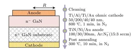
Fig. 1. Schematic view of the vertical GaN SBD temperature sensors with different anode radii(R). The corresponding main fabrication processes are also listed.
3. Results and discussions
The typicalI-V-Tcharacteristics of SBD with an anode radius of 55µm were recorded,as shown in Fig.2(a). TheVonextracted by linear fitting the forward region is about 0.47 V,which is consistent with previous reports.[14,17]In addition,theI-V-Tcurves show a zero-temperature coefficient(ZTC)point. Obviously, the variation of current versus temperature are different in the bias regions above and below the ZTC point (approximately 0.6 V). For the small forward voltage(VF) region (below ZTC point), the voltage at a specific current value decreases gradually with the increasing temperature(negative coefficient). Noticeably, above the ZTC point (relatively highVFregion),the voltage at a specific current value increases gradually with the increasing temperature (positive coefficient).
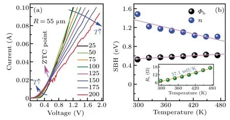
Fig.2. The I-V-T characteristics(a)of vertical GaN SBD with an anode radius of 55µm. (b)The relationship between key parameters and temperature.
Theoretically, theI-V-Tcurves of the SBD follow the thermal emission (thermionic emission, TE) model. The forward currentIDunderVF>3kT/qreads[17]
TheVFis then solved as
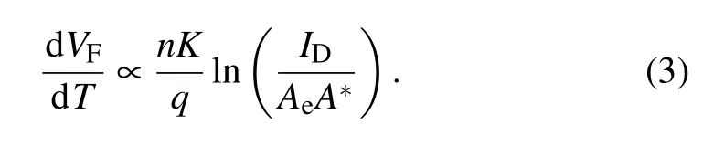
whereAe,T,q,n,k,A∗andRsare the Schottky anode area,Kelvin temperature, electronic charge, ideality factor, Boltzmann constant, Richardson constant (26.9 A·cm-2·K-2in our calculation) and series resistance, respectively. Based on Eq.(2),the key parameters(Φb,n,andRs)of the SBD versus temperature with an anode radius of 55µm are fitted and plotted in Fig.2(b). It is demonstrated that theΦbincreases from 0.52 eV to 0.62 eV linearly with the increasingT, while thendecreases from 1.4 to 1.0 linearly. In addition,we also find that theRsincreases from 7.3 Ω to 17.2 Ω with temperature in a slope of 57.1 mΩ/K.The variation ofΦbandnversus temperature are not consistent with the TE model,in which those values should be constants. The possible reason is attributed to the spatial fluctuation ofΦbat interface,namely,the barrier height inhomogeneous effect.[19]The carrier at relatively high temperature gains more energy and then overcomes the high barrier patch,resulting in a high average barrier height.
To evaluate the effect of anode radius on the electrical properties,theI-V-Tcharacteristics of SBDs with anode radii of 70µm and 85µm are shown in Figs.3(a)and 4(a),respectively. TheI-V-Tcharacteristics of both diodes are comparable with that of the small anode one,except the forward voltage that reaches the compliance current. By fitting theI-V-Tcurves, theΦbof the 70 µm SBD increases from 0.61 eV to 0.67 eV,while thendecreases from 1.2 to 1.0 linearly with the increasingT(Fig.3(b)). TheΦbof the 85µm SBD increases from 0.56 eV to 0.67 eV, while thendecreases from 1.2 to 1.0 linearly with the increasingT(Fig. 4(b)). Those values and the variation trends are comparable to each other, implying that other factors are the root causes.It is worth noting that the slopes ofRsare 37.1 mΩ/K and 26.3 mΩ/K for the 70µm(inset of Fig. 3(b)) and 85 µm (inset of Fig. 4(b)) diodes, respectively.This indicates that theRspresents an obvious effect at the voltage region above the ZTC point.
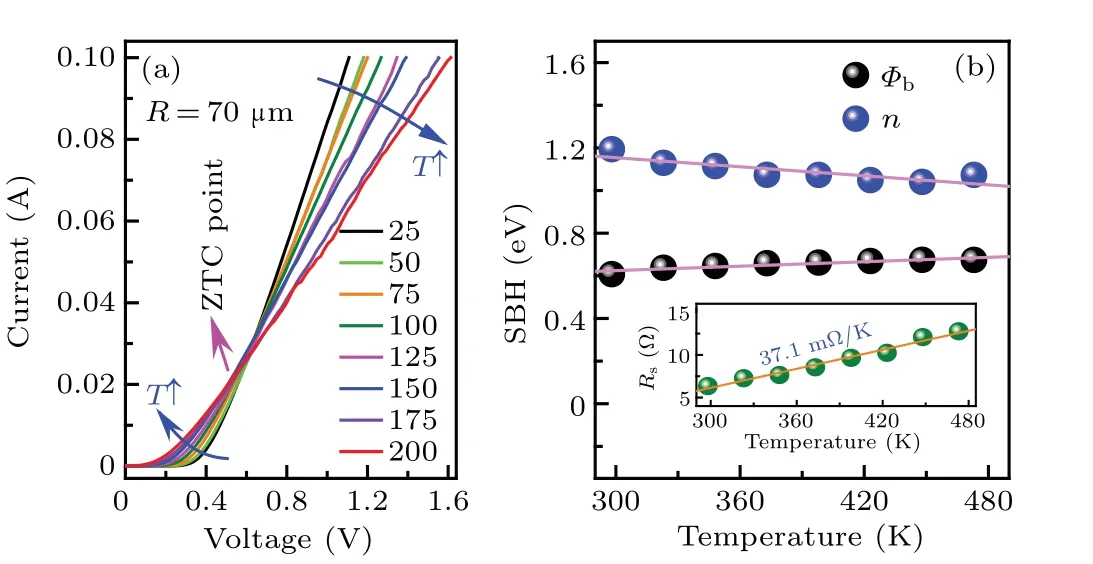
Fig.3. The I-V-T characteristics(a)of the vertical GaN SBD with an anode radius of 70 µm. (b) Relationship between key parameters and temperature.
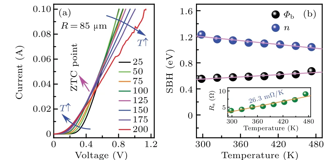
Fig.4. The I-V-T characteristics(a)of the vertical GaN SBD with an anode radius of 85 µm. (b) Relationship between key parameters and temperature.
The relationship between forward voltage and temperature is commonly used for determining the sensitivity. Furthermore, the sub-threshold region is preferable for temperature sensing application due to the relatively small power loss. When we choose a specific current(1×10-5,1×10-4,5×10⁻⁴,or 1×10⁻³A in our experiment),the corresponding forward voltage on theI-V-Tcurves shifts negatively with the increasing temperature (Fig. 5(a)). The variation of this forward voltage versus temperature is then plotted in Fig. 5(b).Under four selected current levels,the corresponding forward voltage decreases with increasing temperatures,implying that the slope is negative(Fig.5(b)). Based on the absolute slope of the fitting line, the measured sensitivitiesSmare deduced to be 1.19, 1.2, 1.14, and 1.13 mV/K at 1×10⁻⁵, 1×10-4,5×10-4, and 1×10⁻³A, respectively. Based on Eq. (2),theVFis determined by three main parts. Firstly, we confirm that the productionnΦbshows slight dependence on temperature (Fig. 6(a)), which is ascribed to the opposite variation trends ofΦbandn. Secondly, the voltage drop contributed by theRs(I×dRs/dT)is smaller than 0.05 mV/K due to the small current in sub-threshold region. In addition, the nonlinear part of lnTcan also be ignored in relatively small temperature range.[20]Hence,the sensitivity dVF/dTis correlated with the current densityID/Aeas
Therefore,the sensitivity is mainly determined by the ideality factorn,current levelIDand anode areaAe,but is not related with the wafer structure and diode geometry(circular, finger,dot,etc.).The above discussion is confirmed by the decreasing trend of sensitivity versus current level,which is proportional to the logarithms of current density (Fig. 6(b)). Because an ideal SBD follows the TE model, the change of anode material(variation inΦband reverse leakage current)has no direct effect on the sensitivity. In addition,although the interface reaction for the metal anode on GaN generates a relatively highernand contributes to the sensitivity,the degradation of reliability is unsuitable for high temperature applications.
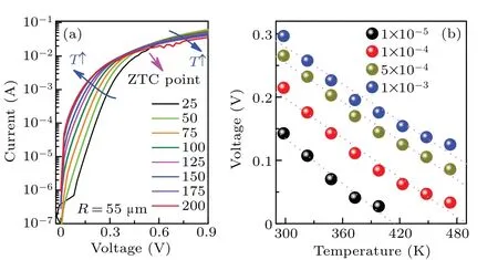
Fig.5. (a)The sub-threshold region I-V-T characteristics of the vertical GaN SBD with an anode radius of 55µm.(b)The VF-T relationship at different current levels.
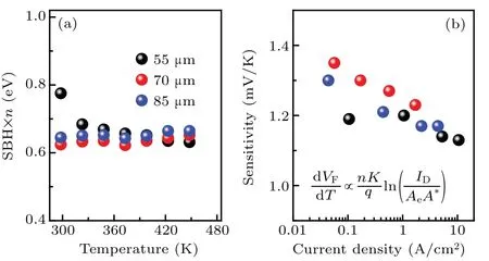
Fig. 6. (a) The production of SBH and n versus temperature. (b) The relationship between sensitivities and current density.
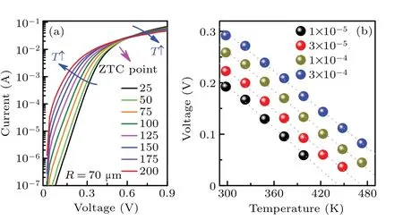
Fig.7. (a)The sub-threshold region I-V-T characteristics of the vertical GaN SBD with an anode radius of 70µm.(b)The VF-T relationship at different current levels.
To evaluate the effect of anode area on the sensitivity,the sub-threshold region ofI-V-Tcharacteristics for the SBDs with anode radii of 70 µm and 85 µm are also plotted in Figs.7(a)and 8(a),respectively. Then,the correspondingVFTrelationships at different currents with the fitting line are plotted in Figs. 7(b) and 8(b), respectively. Obviously, good linearity can be observed for all theVF-Tcurves,and the deduced sensitivities are summarized in Fig. 6(b). On the one hand, the production ofΦbandnshows slight dependence on temperature (Fig. 6(a)). On the other hand, the voltage drop contributed by theRs(SR, the production of dRs/dTand current)is smaller than 0.04 mV/K.Therefore,the sensitivity is also proportional to the logarithms of current density(Fig.6(b)).Therefore,when the sensor works at a specific current(sub-threshold region),a relatively larger anode area helps to realize a smaller current density and to obtain a higher sensitivity.
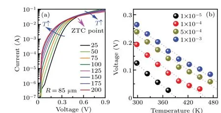
Fig.8. (a)The sub-threshold region I-V-T characteristics of the vertical GaN SBD with an anode radius of 85µm.(b)The VF-T relationship at different current levels.
Unlike the sub-threshold region,the voltages at a specific current increase with the increasing temperature in the fully turn-on region,showing a positive slope above the ZTC point(Fig.9(a)). At a current of 80 mA,theSmvalues are deduced to be 3.81 mV/K, 2.04 mV/K, and 1.46 mV/K for the SBD with anode radii of 55 µm, 70 µm, and 85 µm, respectively.However,theSRvalues contributed by theRsare calculated to be 4.56 mV/K,2.97 mV/K,and 2.1 mV/K(Fig.9(b)). Therefore,theSmis dominated by theSRin this region. We realize that the series resistance degrades the temperature error and linearity,[13]implying the fully turn-on region is not suitable for temperature sensor application. It is worth noting that a larger anode area helps to decrease theRsand to improve the sensing ability.
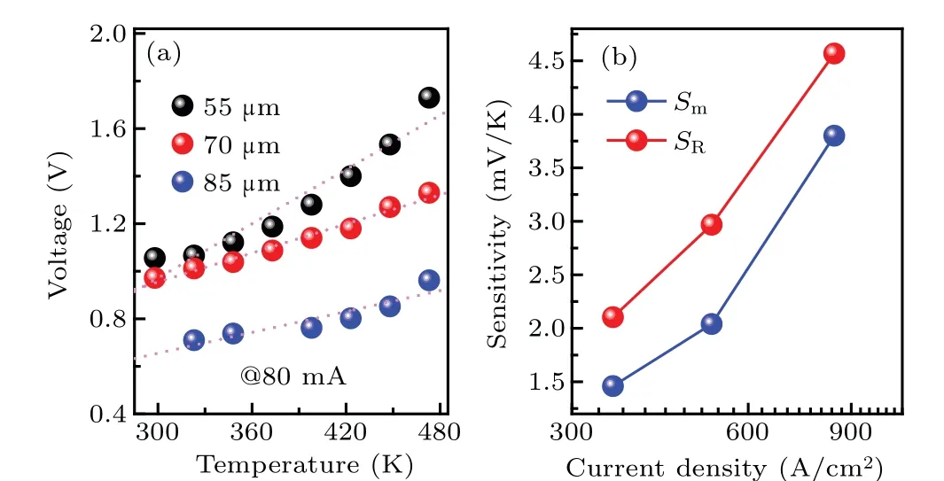
Fig. 9. (a) The VF-T relationship in fully turn-on region for the SBD with different anode radii. (b) The relationship between sensitivities and current density.
4. Conclusions
In summary, we have fabricated vertical GaN SBD temperature sensors using a thermally stable TiN anode. Based on theI-V-Tcharacteristics, the effect of anode area on the sensitivity is investigated. It is demonstrated that theI-V-Tcharacteristics are comparable to each other for the diode with different anode areas, presenting a ZTC point and a typical barrier inhomogeneous behavior. In addition,theRsincreases with temperature in slopes of 57.1 mΩ/K, 37.1 mΩ/K, and 26.3 mΩ/K for 50µm,70µm,and 85µm diodes,respectively.When the voltage is below the ZTC bias point(sub-threshold range), the forward voltage decreases linearly versus temperature with a negative slope. The sensitivity deduced from the absolute value of slope is dominated by the current density,which follows the TE model. A large anode area helps to enhance the sensitivity at the same current level. When the voltage higher than the ZTC point (fully turn-on range), the forward voltage increases linearly with temperature in a positive slope. Then, the contribution of series resistance dominates the sensitivity. Under this condition,a larger anode area helps to decrease the series resistance and to improve the sensing ability.
Acknowledgements
The author Ji-Yao Du thanks Professor Hongwei Gao,the Dean of School of Automation and Electrical Engineering,for providing the post-doctoral position and the corporation opportunity with Tokushima University.
This work was supported by the Scientific Research Support Foundation for Introduced High-Level Talents of Shenyang Ligong University (Grant No. 1010147000914)and the Science and Technology Program of Ningbo (Grant No.2019B10129).
猜你喜欢
Chinese Physics B(2022年10期)2022-10-26
Plasma Science and Technology(2022年8期)2022-09-14
意林彩版(2022年1期)2022-05-03
船电技术(2022年3期)2022-03-19
诗潮(2021年11期)2021-11-24
红河学院学报(2021年4期)2021-11-19
时代风采(2019年7期)2019-12-14
新农村(2017年20期)2017-09-28
今古传奇·故事版(2016年23期)2017-01-12
故事会(2016年21期)2016-11-10

- Chinese Physics B的其它文章
- Quantum walk search algorithm for multi-objective searching with iteration auto-controlling on hypercube
- Protecting geometric quantum discord via partially collapsing measurements of two qubits in multiple bosonic reservoirs
- Manipulating vortices in F =2 Bose-Einstein condensates through magnetic field and spin-orbit coupling
- Beating standard quantum limit via two-axis magnetic susceptibility measurement
- Neural-mechanism-driven image block encryption algorithm incorporating a hyperchaotic system and cloud model
- Anti-function solution of uniaxial anisotropic Stoner-Wohlfarth model