
Effect of Cu doping on the secondary electron yield of carbon films on Ag-plated aluminum alloy
2022-04-12 03:45TiancunHu胡天存ShukaiZhu朱淑凯YananZhao赵亚楠XuanSun孙璇JingYang杨晶YunHe何鋆XinboWang王新波ChunjiangBai白春江HeBai白鹤HuanWei魏焕MengCao曹猛ZhongqiangHu胡忠强MingLiu刘明andWanzhaoCui崔万照
Chinese Physics B 2022年4期
关键词:胡天
Tiancun Hu(胡天存) Shukai Zhu(朱淑凯) Yanan Zhao(赵亚楠) Xuan Sun(孙璇) Jing Yang(杨晶)Yun He(何鋆) Xinbo Wang(王新波) Chunjiang Bai(白春江) He Bai(白鹤) Huan Wei(魏焕)Meng Cao(曹猛) Zhongqiang Hu(胡忠强) Ming Liu(刘明) and Wanzhao Cui(崔万照)
1Key Laboratory for Physical Electronics and Devices of the Ministry of Education,School of Electronic Science and Engineering,Xi’an Jiaotong University,Xi’an 710049,China
2National Key laboratory of Science and Technology on Space Microwave,China Academy of Space Technology(Xi’an),Xi’an 710100,China
3Electronic Materials Research Laboratory,Key Laboratory of the Ministry of Education&International Center for Dielectric Research,School of Electronic Science and Engineering,Xi’an Jiaotong University,Xi’an 710049,China
Keywords: copper-doped carbon,secondary electron yield,microwave devices,surface roughness
1. Introduction
High-power microwave components are one of the core payloads in spacecrafts and satellites.[1-4]However, the multipactor effects become more and more destructive in space as the microwave devices become miniaturized and integrated.The multipactor effects can increase the surface temperature of microwave components and the noise level of the microwave devices which decreases the output power levels.[5,6]In more serious cases, permanent failures of microwave components may occur. Therefore, improving the multipactor threshold of microwave components or avoiding the multipactor has become a key research topic,[7-9]which should be considered in designing satellite systems with high-power microwave components.
Generally,the multipactor effect is strongly related to the secondary electron yield (SEY) of the materials.[10-12]The two most commonly used methods to suppress SEY effects are micro-trapping structure surface[13-17]and surface coating with low SEY materials.[8]Yeet al.reduced the maximum secondary electron emission coefficient(δmax)by 60%by fabricating the triangular raised structures.[18]Baiet al.prepared porous anodic alumina films with various hole sizes on aluminum alloy substrates,[19]resulting in an obvious inhibiting effect in the SEY coefficient.However,the signal transmission becomes worse and energy loss also increases when the operations are applied to high power microwave devices. Heet al.sputtered platinum film(100 nm)on the surface of silver plating aluminum alloy samples,[20]in which the maximum SEY coefficient decreased from 2.40 to 1.77. In addition,TiN2thin films were prepared on monocrystalline silicon and glass by RF magnetron sputtering,[16]and it not only efficiently suppresses the SEY coefficients but also improves the threshold value of multipactors of components.
The amorphous carbon (C) film[5,7,21-23]is a metastable material with coexistence of diamond phase and graphite phase,[24-27]which could suppress the SEY effect through a simple coating process. Copper metals also have small secondary electron emission coefficients and their electrical conductivities satisfy the requirements of microwave components.[28]In this study, copper doped carbon films are sputtered on silver-plated aluminum alloy substrates. Then,the secondary electron yield characteristics of the C/Cu composite films are systematically analyzed by the x-ray photoelectron spectroscopy and scanning electron microscopy. In addition, sp2/sp3hybrid bonds of the C/Cu composite films are presented to reveal the physical mechanism by Raman spectroscopy.[24,28-30]
2. Experiment
Undoped carbon films and Cu films were deposited by a magnetron sputtering system at argon pressure of 1.5 Pa with microwave power at 150 W and 70 W,respectively. Cu-doped C films with different compositions were prepared by controlling the sputtering powers, as shown in Table 1. Two experimental samples of different sputtering systems were obtained finally. The amount of metal nanoparticles deposited on the surface of the film is different since the growth rates of C and Cu are different. Thus, it is evident that the surface colors of samples obtained by different preparation processes are quite different. The process parameters for the preparation of the C/Cu composite films are listed in Table 1.
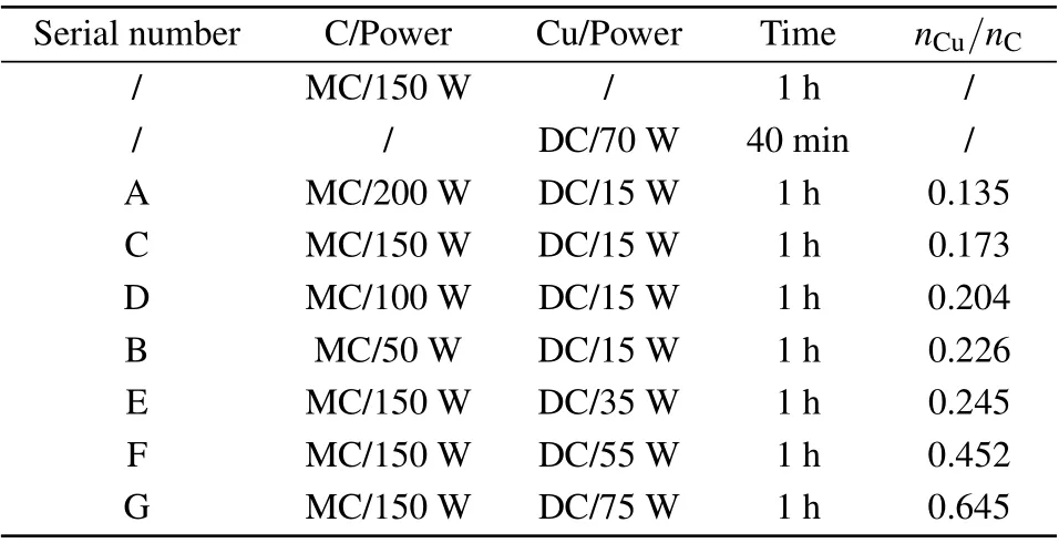
Table 1. Preparation parameters of the Cu-doped carbon films.
3. Results
Firstly, we test the aluminum alloy substrate with pure Cu-plated surface using the SEY characteristic test platform,and the sample is with pure C-plated film. The test results are shown in Fig.1(a). It can be obtained that theδmaxof the Agplated aluminum alloy substrate,the Cu-coated sample and the C-coated sample are 2.522, 1.920, and 1.362, respectively. It is found that the secondary electron yield coefficient (δ) of the substrate surface is significantly reduced after coating,and theδof the sample with a Cu film sputtered on the surface is reduced by about 0.6 compared to the aluminum alloy substrate,which is about 23.79%. In addition,it can be obtained that the primary energy of the maximum (Emax, electronvolt)of the Cu-plated aluminum alloy substrate,Cu-plated sample,C-plated sample is 300 eV,300 eV,200 eV,respectively. The coating process can significantly control the SEY effect.
Secondly,the SEY curves of various C and Cu doping ratios are shown in Fig.1(b). We can find that the Cu-doped and C-based nano-films can suppress the SEY. With the increase of the metal Cu doping ratio, theδmaxcan be reduced from 1.69 to 1.53. The best suppression effect is the G sample withnCu/nCof 0.645,and itsδmaxis 1.53. Compared with the Agplated Al alloy substrate, its suppression effect is increased by 39.28%, and the suppression effect has been increased by 20.31%compared with the pure Cu sample. The poorer suppression effect is the sample E with annCu/nCof 0.245, and itsδmaxis 1.69. Compared with the Ag-plated aluminum alloy substrate, the suppression effect is increased by 32.94%,and the suppression effect is increased by 11.98% compared with the pure Cu film. The suppression effect of the C/Cu composite film is poor, and theδmaxof all doped samples is higher than 1.36 compared with the pure C film. Based on the data in Fig. 1(a), the least squares polynomial fitting is used to fit the curve ofδmaxwith the C/Cu doping ratio, as shown in Fig.1(c). The SEY coefficient shows a nonmonotonic relationship that increases at first and then decreases with the Cu doping contents.
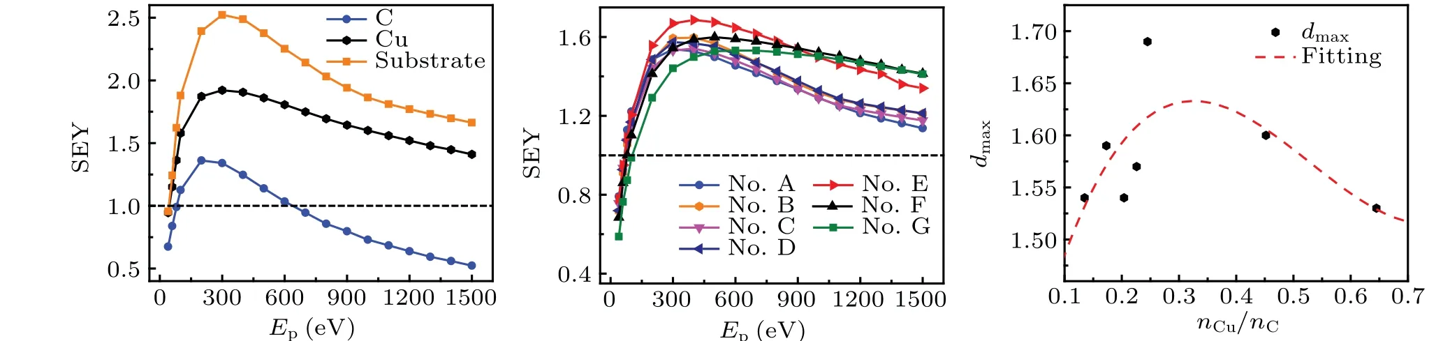
Fig.1. (a) Secondary electron yield curves of aluminum alloy substrate with Ag plating, pure Cu-plated film sample and pure C-plated film sample. (b) The compared secondary electron yield curves of different doping C/Cu samples. (c) The δmax of C/Cu composite film and its fitting trend curve.
The percentages of C and Cu of samples A-G are obtained by using an x-ray photoelectron spectroscopy,as shown in Fig. 2(a). All the samples show the C and Cu elements.Then,the corresponding ratios ofnC/nCuare obtained by peak fitting,as shown in Table 1.
In order to analyze the influence of the structure of the sample on the SEY, we use the field emission scanning electron microscopy (SEM) to characterize the surface and cross-sectional morphology of the B, C and G Cu-doped Cbased nano-film samples,and the inset shows the corresponding sample. According to the sample morphology shown in Figs.2(b),2(c),2(d),when the Cu doping ratio in the C-based composite film is small, such as B (nCu/nC: 0.173) and C(nCu/nC:0.204)samples.The surface of the film sample is flat and the cross-sectional morphology is dense relatively. With the increase of the Cu doping ratio in the composite film,such as sample G (nCu/nC: 0.645), the size of the nano-particles on the surface of the film becomes larger and a large number of nano-particles are precipitated, obvious pores appear,and the surface morphology changes. It can be seen from the cross-sectional morphology that the compactness of the film becomes worse, forming a porous, loose and rough “coralreef”-like structure.
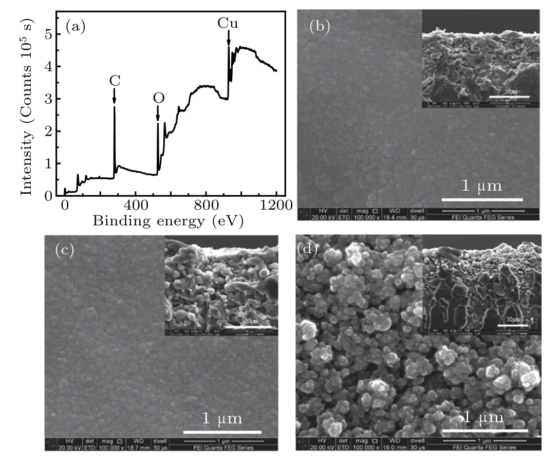
Fig. 2. (a) The XPS of the C/Cu composite films. Surface morphology of C/Cu composite films with different Cu contents. (b) Sample B nCu/nC:0.173. (c)Sample C nCu/nC: 0.204. (d)Sample G nCu/nC: 0.645.
The reasons for the above-mentioned changes in sample morphology seem to be that, on the one hand, the change of sputtering power during film growth not only affects the change of metal doping ratio,but also changes the energy and intensity of incident ions,thereby affecting the structure of the film. On the other hand,the surface of the film forms clusters with small scale and loose structure because there is no chemical bond between Cu and C atoms. The Cu nanoparticles in the film cause crystal lattice defects through dislocation slippage, etc., and then make up a series of “trap” structure. In addition,the Cu nanoparticles serve as a buffer material in the film,which can significantly reduce the internal stress and improve the film-base bonding force to a certain extent.
Since the samples F and G are seriously oxidized,Raman spectroscopy could not be obtained because of the obvious fluorescence interference. Therefore, Raman spectroscopy was performed on samples A-E,as shown in Fig.3(a). The analysis of Raman spectroscopy is important to gain a better understanding how the Cu doping will affect sp2and sp3hybridization types of coordination bonds. Through the data processing method of peak fitting,the Raman spectra of samples A-E are analyzed,respectively. First,two different Gaussian peaks are obtained as shown by the red curve (D) near 1390 cm-1and the green curve (G) near 1585 cm-1. By sorting out the Raman data of samples A-E, the information such as the half width of the G peak is given in Table 3. It can be obtained that with the increase of the metal Cu doping ratio,ID/IGshows a monotonous decreasing trend, and the change trend of the peak position of the G peak is first increasing, then decreasing,and then increasing again,as shown in Fig.3(b).GFWHMis the overall increasing trend at the same time,which includes rise and fall alternating as shown in Fig.3(c).
Fig.3. (a)Raman spectrum of samples A-E.(b)The change trend of ID/IG and G peak position. (c)The change trend of GFWHM.

Table 2. Raman spectroscopy analysis of the C/Cu composite samples.
As can be seen from Fig.3(b),with the change of doping ratio,ID/IGdecreases from 3.917 to 2.766,a drop of 29.38%.The peak position of the G peak increases from 1583.42 cm-1to 1589.58 cm-1, and moves about 6 cm-1to the high wave number range. The peak intensity ratio of the D peak to the G peak first decreases from 3.917 to 3.605 and then increases to 3.801 when the doping ratio is less than 0.245, a decrease of 2.96%; the peak position of the G peak first increases from 1583.42 cm-1to 1585.79 cm-1and then decreases to 1581.87 cm-1,a decrease of about 0.98%,indicating that the sp2hybrid bond content in the C-based composite film is generally decreasing. As shown in Fig.3(c), when the doping ratio is less than 0.245,theGFWHMincreases from 127.24 cm-1to 129.05 cm-1, the overall increase is 1.42%,and the degree of disorder of the film decreases, indicating that the sp2hybrid bond content of C-based composite film is reduced overall.[6]Comprehensive analysis of the reasons for the above phenomenon,firstly,the energy of the sputtered metal ions can be injected into the C film to promote the conversion of sp2bonds to sp3bonds,and result in increasing the content of sp3bonds in the film.However,as shown in Table 1,the sputtering power of Cu is 15 W for samples A,B,C,and D,which is not enough to damage the structure of the sp3hybrid bond. Secondly,the temperature of the film surface is not enough to promote the conversion of sp3bonds to sp2bonds in the film. Thirdly, more Cu nanoparticles may be precipitated after the sputtering process, since Cu has little solid solubility in the amorphous C network, such as sample F. Here, the sputtering power of Cu is 55 W and 75 W for samples F and G,respectively. Thus,there would exist more nanoparticles in the larger Cu doping samples.
Considering the above analysis, the mechanism can be summarized as follows: Firstly,according to the sample morphology, with the increase of Cu doping ratio, the size and number of the nanoparticles becomes larger on the surface of the film, and then obvious pores appear. It can be seen that the compactness of the film becomes worse, forming a porous, loose and rough “coral-reef”-like structure. Such a“trap” structure can effectively inhibit the secondary electron emission to some extent. Secondly, due to the small solid solubility of Cu in the amorphous carbon network, more Cu nanoparticles will be precipitated. Moreover,Cu is easy to be oxidized in the atmosphere. The generated metal oxide has a higher secondary electron emission coefficient. Thus, the inhibition effect of secondary electron emission is poor. Thirdly,the number of sp2hybrid bond decreases as the increase of the Cu doping ratio in the prepared films. The lower sp2content would lead to fewer free electrons,and the excited secondary electrons in the full band are less likely to collide with free electrons as they move toward the surface. Therefore,the escape ability is improved, and the suppression of SEY is reduced. The interaction of the three conditions makes the SEY coefficient increase first and then decrease.
4. Conclusion
In summary, various Cu-doped carbon films have been sputtered by controlling the sputtering power and the depositing time, and the mechanism of secondary electron suppression is analyzed. The lowestδmaxcan reach 1.53 in the Cu doping sample (nCu/nC, 0.645), and its suppression effect is increased by 39.28% compared with the Ag-plated Al alloy substrate. It is found that SEY increases with Cu contents due to the oxidation susceptibility of Cu and the decrease of sp2bonds. However, the addition of Cu increases the roughness and the number of charge traps of the carbon film,which efficiently reduces the SEY.Low SEY in Cu-doped carbon films deposited on Ag-plated aluminum alloy is potentially useful for applications in high power microwave components.
Acknowledgements
This work was supported by the National Key Laboratory Foundation (Grant Nos.2018SSFNKLSMT-04,614241101010117 and 6142411191110) and the National 111 Project of China(Grant No.B14040).
猜你喜欢
心理学报(2022年2期)2022-02-15
今日农业(2021年12期)2021-11-28
北京大学学报(自然科学版)(2021年3期)2021-07-16
民间故事选刊·上(2019年11期)2019-12-10
心理学报(2018年12期)2018-12-10
传奇·传记文学选刊(2018年6期)2018-06-21
长江文艺·好小说(2018年3期)2018-03-21
领导文萃(2015年16期)2015-09-09
党史文苑(2015年7期)2015-05-18
- Chinese Physics B的其它文章
- Quantum walk search algorithm for multi-objective searching with iteration auto-controlling on hypercube
- Protecting geometric quantum discord via partially collapsing measurements of two qubits in multiple bosonic reservoirs
- Manipulating vortices in F =2 Bose-Einstein condensates through magnetic field and spin-orbit coupling
- Beating standard quantum limit via two-axis magnetic susceptibility measurement
- Neural-mechanism-driven image block encryption algorithm incorporating a hyperchaotic system and cloud model
- Anti-function solution of uniaxial anisotropic Stoner-Wohlfarth model