
Micro thermoelectric devices: From principles to innovative applications
2022-04-12 03:47QiulinLiu刘求林GuodongLi李国栋HangtianZhu朱航天andHuaizhouZhao赵怀周
Chinese Physics B 2022年4期
关键词:航天
Qiulin Liu(刘求林) Guodong Li(李国栋) Hangtian Zhu(朱航天) and Huaizhou Zhao(赵怀周)
1Beijing National Laboratory for Condensed Matter Physics and Institute of Physics,Chinese Academy of Sciences,Beijing 100190,China
2School of Physical Sciences,University of Chinese Academy of Sciences,Beijing 100049,China
3Songshan Lake Materials Laboratory,Dongguan 523808,China
Keywords: thermoelectric microdevices,contact impedance,local temperature control,energy harvesting
1. Introduction
Thermoelectric(TE)technology can convert heat directly into electricity and vice versa.[1,2]The basic principles of conversion can be explained by the Seebeck effect and Peltier effect,both of which originate from the difference of carrier energy in materials.In recent years,thermoelectrics has attracted considerable interest due to the significantly improved performance of thermoelectric materials and innovative applications.The conversion efficiency of thermoelectric materials is determined by a dimensionless figure of merit zTthat is defined as zT=(α2σ/κ)T,whereα,σ,κ,andTare the Seebeck coefficient,electrical conductivity,thermal conductivity,and absolute temperature,respectively.[3]Clearly,to reach a high figure of merit, a large Seebeck coefficientα, a high electrical conductivityσ,and a low thermal conductivityκare required.[4,5]In addition to the aspect of thermoelectric materials,more factors should be considered for the device design to reach the prescribed performance (conversion efficiency for TEGs and coefficient of performance for TECs), for instances, the geometric configuration of thermoelectric pairs,thermal and electrical contact resistances,and so on.[6]
Advances in modern technology have consistently pushed the miniaturization of electronic devices or systems and brought more opportunities for commercial profit.[7]The traditional evolutionary engineering effort (i.e., cutting process)to reduce size suffers from inefficient delivery and/or precision limit of several hundreds of micrometers. The field of microelectromechanical systems(MEMS)represents great efforts to radically transform the scale, performance, and cost of systems.[8,9]Micro-thermoelectric devices (µ-TEDs),schematically shown in Fig. 1, are typically Π-structured formed by connecting micro-scale N-type and P-type thermoelectric legs of high-aspect-ratio structure with plate-shaped electrodes.[10,11]To facilitate the application ofµ-TEDs, the device fabrication technologies need to be compatible with the material fabrication methods. Microfabrication technology for creatingµ-TEDs can be roughly divided into masked and maskless types. LIGA and direct ink writing (DIW) are the representative methods that have successfully been used to prepareµ-TEDs,which are also demonstrated in detail in the following section.
The micro-thermoelectric coolers (µ-TECs) are essentially heat pumps dissipating heat in a direction opposite to natural heat transfer, which makes them particularly useful for local temperature control in a range of emerging systems,such as on-chip lasers,microfluidic chips,and wearable electronics.[12]Heat dissipations based on air-cooling techniques are now reaching their limits.[13]Current cooling technologies based on conduction and convection can potentially achieve high power cooling levels by using novel high thermal conductivity materials such as BAs crystals[14,15]or advanced heat exchangers such as microchannels.[16]However,they cannot provide site-specific or on-demand localized cooling of high heat flux regions. The µ-TECs offer the benefits of the scalable structure,silent operation,and reliable temperature control, which make them suitable alternatives for the above-mentioned application scenarios.
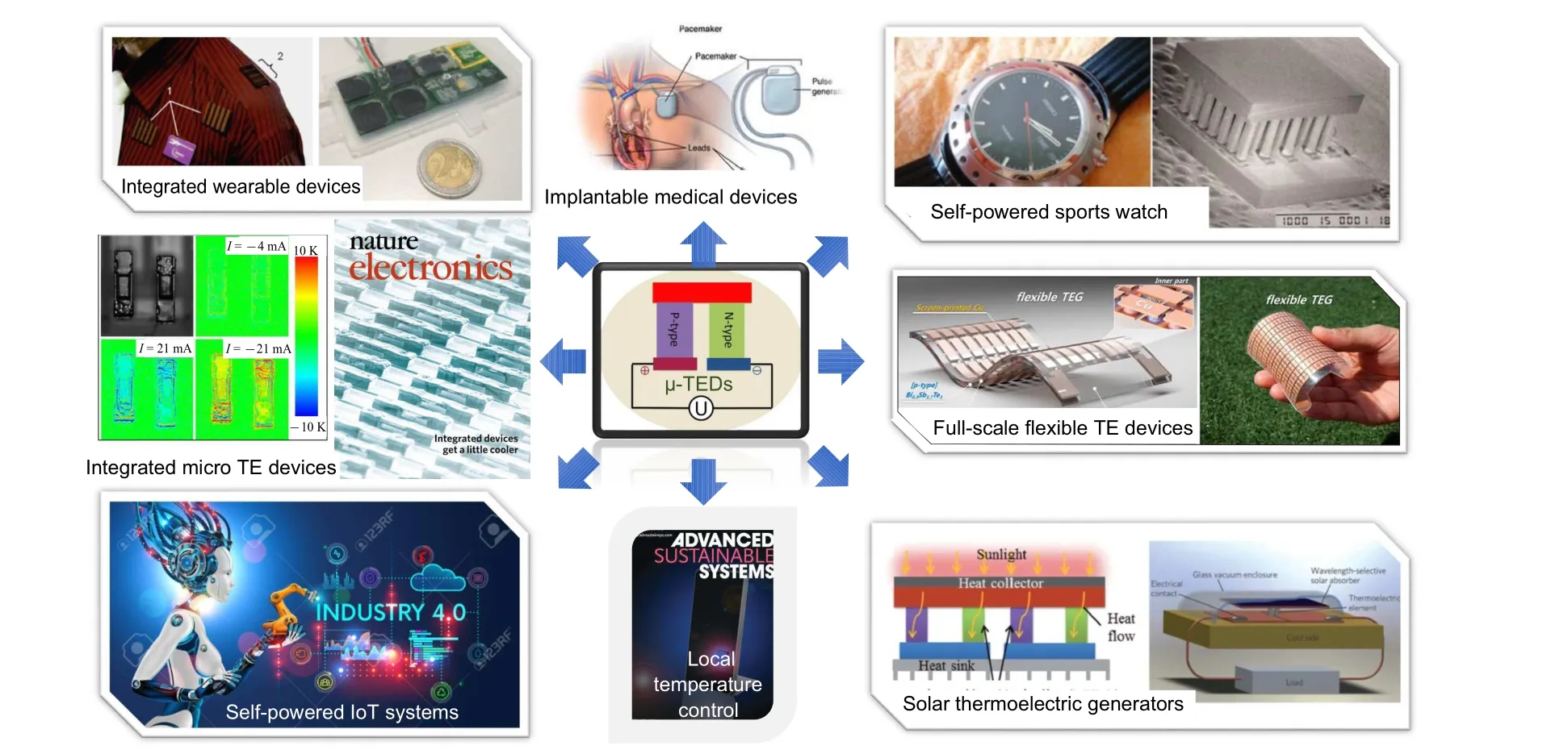
Fig.1. An overview map ofµ-TEDs covering state-of-the-art fabrication technologies, frontier applications, and strategies for improving energy utilization. Reproduced with permission from Refs.[20,23-25]. Health monitoring,wearable electronics,local temperature control as well as the internet of things are only parts of the potential areas ofµ-TEDs.
On the other hand, micro-thermoelectric generators (µ-TEGs)are devices across which a temperature difference generates a voltage difference, which can be used as power supplies or temperature sensors. The energy consumption of microdevices (such as IoT nodes, actuators, and microcontrollers) is usually tiny and continuously diminishing.[17,18]Powering these devices typically requires micro batteries or very long cables connected with electrical grid.[19]Obviously,both methods are not very suited for powering these devices due to their service life and cost. µ-TEDs,with advantages of safety,long-lasting,and maintenance-free,are thus considered as promising alternatives to avoiding these problems. Moreover, combining innovative heat collection and/or dissipation design,µ-TEGs could efficiently utilize thermal energy,[20-22]which are further presented in Figs.1 and 9.
Up to now, there have been several comprehensive reviews or books that introduced the thermoelectric materials,overall principle, and existing applications of bulk thermoelectric devices.[26-29]However,in this review,we mainly focus on the fundamentals of micro-thermoelectric devices and their recent developments. Starting from a general introduction on the core principles of thermoelectric devices, which provides deep understanding of thermoelectric conversion and the relationship between device performance and engineering schemes (including the geometry of TE legs, connecting schemes,various interfaces). Next,several typical device fabrication methods are introduced. The thin-film material preparation and microfabrication technology are relatively mature,but the device fabrication methods need to be balanced with the material preparation technology.In this part,we first introduce the main methods of preparing thermoelectric thin films and then introduce the representative device integration methods. Finally, innovative applications are introduced based on the characteristic ofµ-TEDs.
2. Figure of merit and device design principles
2.1. Ideal thermoelectric devices
Ideal thermoelectric devices follow a set of design principles determined by thermoelectric properties and geometry features of thermoelectric pairs. An ideal TE device means that the thermal resistance and resistance between the TE leg and the electrode are not considered,and its principle can provide an essential guide for the actual TE device. The dimensionless figure of merit of zT,defined as zT=(α2σ/κ)T,has been used to evaluate the thermoelectric properties of the materials. The question will be discussed in this part: How to optimize the performance of a thermoelectric device made of a given thermoelectric material?
The device figure of meritZT=(α2p,nT)/(RK)can be responsible for a complete thermoelectric device,[30]in whichαp,n,R, andKare the overall device Seebeck coefficient, the electrical resistance and thermal conductance of the P-type and N-type thermoelectric elements. In order to optimize the performance of the device,and so minimize the product of electric resistance and thermal conductance,the following relationship should be followed:

whereAp,Lp,ρp,κp,An,Ln,ρn,κnare the cross-section area,length,electrical resistivity,and thermal conductivity of P-type and N-type elements,respectively.
Thermoelectric generators are typically designed to maximize their device efficiencyηor output powerP. The efficiencyηdepends on the Carnot cycle efficiencyηc=

whereT2,T1,andAare the temperatures of hot and cool ends of TE pairs, and the total cross-section area of TE pairs, respectively.Decreasing the TE pairs lengthLdirectly decreases the internal resistance of the complete devices, which in turn increases the maximum output power. Therefore, compared with bulk thermoelectric devices, µ-TEDs with length in micrometer scale could in principle output higher power density.

2.2. Real thermoelectric devices
However, in the real application of thermoelectric devices, we have to consider the influence of electrode materials,in terms of the additional electrical and thermal resistance of electrode,and the interface impedance between TE element and electrode materials. We now consider a single thermocouple to study the impacts of the thermal and electrical contact resistances for thermoelectric generators. As shown in Fig. 2(a), N-type and P-type TE legs are connected in series by highly conducting metal strips to form a thermocouple. A heat balance at each section is given by
whereQ1andQ2are the heat absorbed at the hot junction and released at the cold side,respectively;T1,T1c,T2c,andT2are the temperatures of the upper interface of upper electrode,upper interface of TE legs, lower interface of TE legs, and the lower interface of lower electrode, respectively;AcandRare the cross-section area of a single TE leg and the internal electrical resistance, respectively. The thermal contact resistance(in units of K·m2·W-1)θc=θi+lc/kc,includes two parts,interface thermal resistivityθiand the contribution of electrodes resistancelc/kc(lcis thickness of electrode),and the electrical resistance(in units of Ω)R=R0+Rcalso includes two parts,i.e., internal resistance of thermoelectric legsR0and electrical contact resistanceRc. It should be mentioned that we only consider the contact resistance between TE legs and electrode while the electrode resistance is neglected in the model, the rationality of which will be verified in the following analyses.
For convenience,we use two notations and definitions as follows:[31]
in whichr(in units of m)is defined as the ratio of the electrical contact resistivityρc(in units of Ω·m2) and the electrical resistivity of the thermoelectric materialsρ;c(in units of m)defined as the ratio of the interfacial thermal resistivityθc(in units of K·m2·W-1)and the thermal resistance of thermoelectric materialsθ=k-1. Therefore, the internal electric resistance can be expressed asR=R0(1+r/l).
Assuming the thermoelectric materials have anZ¯Tc=Z(T1c+T2c)/2 value of 1, equation(5)could be further simplified. In general, the most concerned operating condition is the maximum output power. Thus, electric currentI=αp,n(T1c-T2c)/2Ris used for the calculations. Under the conditions described above,the relationship between the real and ideal temperature differences can be obtained as

The above conditions give Eq. (8) for the device power dependent on the TE element length, the values ofrandc.The relationships converge to the ideal situation,i.e.,Eqs.(2)and(3),asr=andc=0.
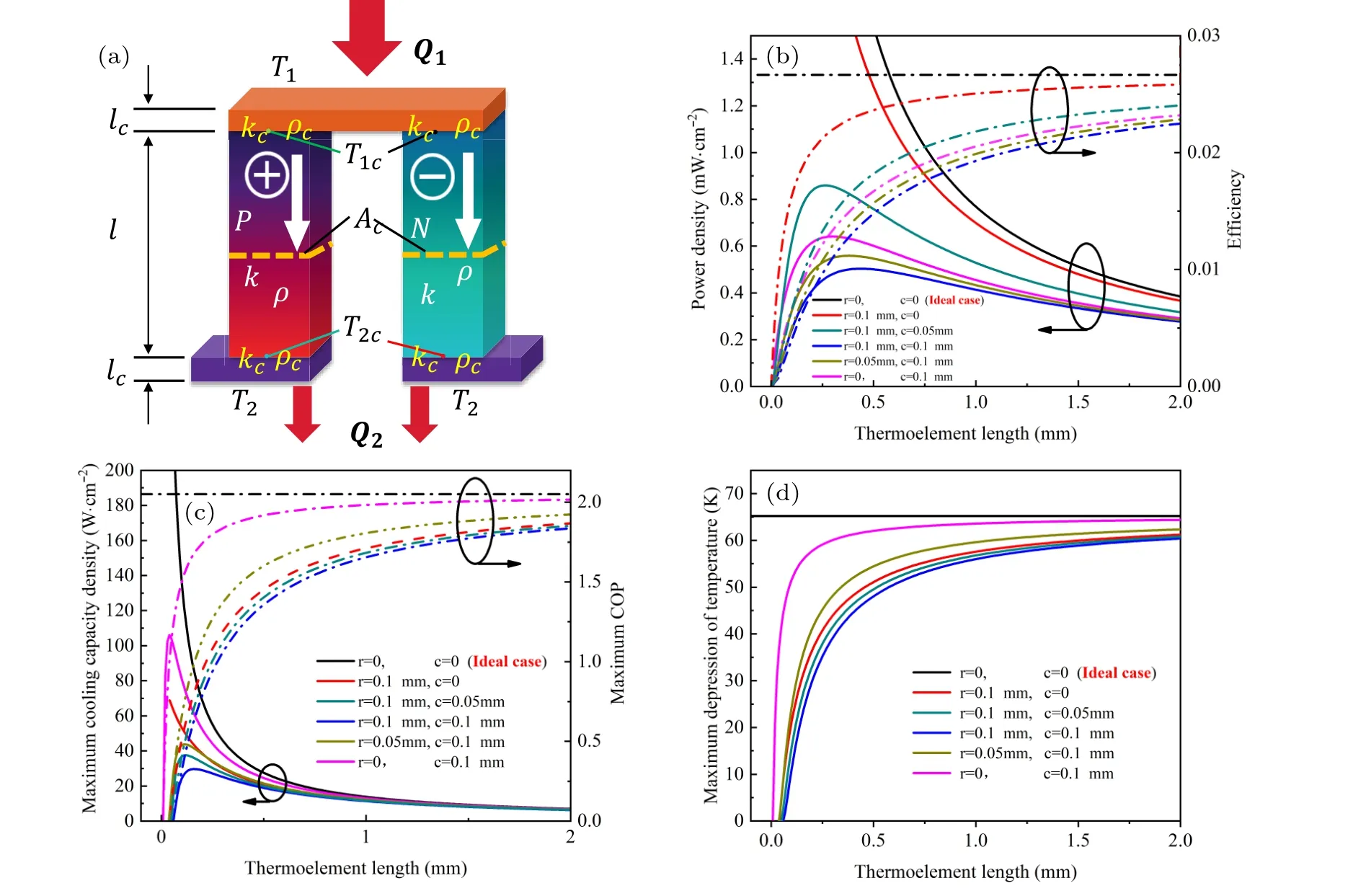
Fig.2. (a)Basic structure of an actual thermoelectric couple. (b)Power density and conversion efficiency as a function of thermoelectric length for different values of r and c. The temperatures of T1 and T2 are 350 K and 300 K in simulation,respectively. (c)Cooling power density and conversion efficiency as a function of thermoelectric length for different values of r and c. (d)Maximum depression of temperature as a function of thermoelectric length for different values of r and c. The absolute value of Seebeck coefficient of 200µV/K,electrical resistivity of 13µΩ·m,thermal conductivity of 1.3 W/(m·K)were used in the simulation for cooling performance.
From these relationships and the corresponding functional images(Fig.2(b)),the maximum power density can be achieved by controlling the length of thermoelectric elements at a certain impendence condition.[32]Moreover, several important conclusions can be drawn: a) The existence of thermal impedance leads to the emergence of the optimal TE leg length. b) The optimum length moves to the larger direction with increasing electric and thermal interface resistance. c)The conversion efficiency shifts from the ideal relationship independent of length to increasing with the increase of length.d) The impact of thermal impedance is greater than that of electrical contact.
Similarly,the cooling performance of real thermoelectric devices is highly dependent on the interface impedance. Figures 2(c)and 2(d)show the maximum capacity density,COP,and depression of temperature for the actual TECs function as thermoelectric pairs length under different values ofrandc.The analysis of actual TECs performance can derive the following main conclusions: a)Similar to TEGs,the existence of thermal impedance leads to the emergence of the optimal TE leg length. b) Different from that TEGs can generator power at any length with any impedance,a certain length threshold is required for the TECs. c)The maximum COP and maximum temperature differences shift from the ideal relationship independent of length to increasing with the increase of length. d)The impact of electrical impedance is greater than that of thermal contact.
3. Micro thermoelectric devices fabrication
3.1. Material aspect
Various techniques have been applied to synthesize highperformance thermoelectric thin films, such as chemical vapor deposition (CVD), physical vapor deposition (PVD), and vapor-liquid-solid growth process.[33]However, these methods are hard to meet the requirement of µ-TEDs because of their inadequate step coverage.[34]In contrast, electrodeposition is a cost-effective and high throughput method to synthesize high-aspect-ratio thermoelectric thin film and compatible with microfabrication processes.[35-37]Moreover, electrodeposition can fabricate films on large and irregular surfaces,which provides the foundation of material synthesis for the broad applicability ofµ-TEDs.
Electrochemical deposition (ECD) usually relies on a three-electrode system composed of the working electrode,the counter electrode, and the reference electrode, which constitute two circuits.[38]The reference electrode and the working electrode form a test circuit,within which an ignorable current is passing through;thereby,the potential of the reference electrode can be considered constant. The working electrode and counter electrode constitute a polarization circuit,in which the current is used to meet the chemical reaction. The potential of the working electrode is measured and controlled based on the potential of the reference electrode(Fig.3(a)).
Understanding the process of electrode reaction aids in understanding the mechanism and kinetics of electrolytic crystal growth, as the physical properties of electrodeposits depend on the process of crystals growth.[39]Thermodynamic conditions can predict whether or not the reaction will occur, while the kinetics determine the chemical reaction rates of the desired reactions and side reactions and subsequently influence the composition,structure,and properties of the reaction product.[40]As shown in Fig. 3(b), the electrode reactions include two basic steps, i.e., the diffusion of the redox species toward the electrode and the electron transfer at the electrode. If the kinetics of electron transfer at an electrode is high-speed, the whole reaction rate depends on the diffusion,and this kind of reaction is termed diffusion-controlled reaction. Conversely,it is called a kinetically controlled reaction.
For a given electrolyte, cyclic voltammograms (CV)curves are usually taken to determine the proper deposition of dissolving potentials. Potential scanning usually leads to current peaks because there are sufficient redox molecules available when the voltage is not too large, while at higher potentials, the current is limited by the diffusion-limited current.The same situation occurs when scanning back in the reverse direction. These phenomena occur in diffusion-controlled and kinetically controlled reactions on metal electrodes. For the diffusion-controlled reaction, the peak current increases with the square root of the scanning rate, but the position is independent of the scanning rate. In contrast, the position of the current peak moves to higher potentials when the scan rate is increased for a kinetically controlled reaction.
For semiconductor electrodes,the CV curves behave very differently. The cathodic reduction reaction always occurs via the conduction band and anodic oxidation reaction via the valence band.[41]The following examples can support this conclusion: 1) The cathodic current due to the formation of H2rises steeply with increasing cathodic potential at the N-type electrode, whereas a tiny current occurs at the P-type electrode. 2) The cathodic current at the P-type electrode is enhanced by light excitation. 3) The anodic current at P-GaAs increases steeply with increasing anodic polarization,whereas a tiny anodic current is found with N-type electrodes. Therefore,most references report that electrodeposited thermoelectric films are always N-type.[42]The cathodic deposition of P-type semiconductors means that the reaction is the minority carrier reaction. The reaction current is very small if the deposited film forms a dense and continuous layer, resulting in big challenges to grow compact and continuous P-type TE films.
Relatively dense P-type TE film made by potentialcontrolled millisecond-pulsed deposition method has been repeatedly reported.[43-45]Christian Schumacheret al. presented an optimization of electrodeposited P-type Sb2Te3thermoelectric films by millisecond potentiostatic pulses in 2012. Figures 3(d) and 3(e) show the morphology of the asfabricated Sb2Te3film fabricated with constant (DC) deposition and pulsed depositionton/toff=10/50 ms, respectively.Clearly, pulse deposition is beneficial to the densification of P-type thin films. In addition to the thermoelectric materials,the interface between TE legs and electrodes significantly affects the device performance. In the manufacturing process of µ-TEDs, after the thermoelectric materials are grown by ECD, the sample can immediately transfer to an electrolyte bath of electrode material, and the metal electrode is electrochemically deposited on the TE pairs which can form an intimate contact between thermoelectric material, as shown in Figs.3(f)and 3(g).
On the other hand, some N-type thermoelectric materials have recently attracted wide attention for their thermoelectric performance approached or even surpassed N-type Bi2Te3such as Ag2Se and GeTe.[46-49]ECD is comparatively less explored among various techniques available for synthesizing or regulating these materials. A single-leg device composed of high-performance N-type thermoelectric materials and metal legs prepared by ECD may be another idea to fabricate high-performance thermoelectric microdevices.Recently,Yanzhong Peiet al. reported a single-leg full-scale thermoelectric device with a conversion efficiency of 14% under a temperature gradient of 440 K based on GeTe-Cu2Te-PbSe alloys,[50]which provides some support for the above idea.
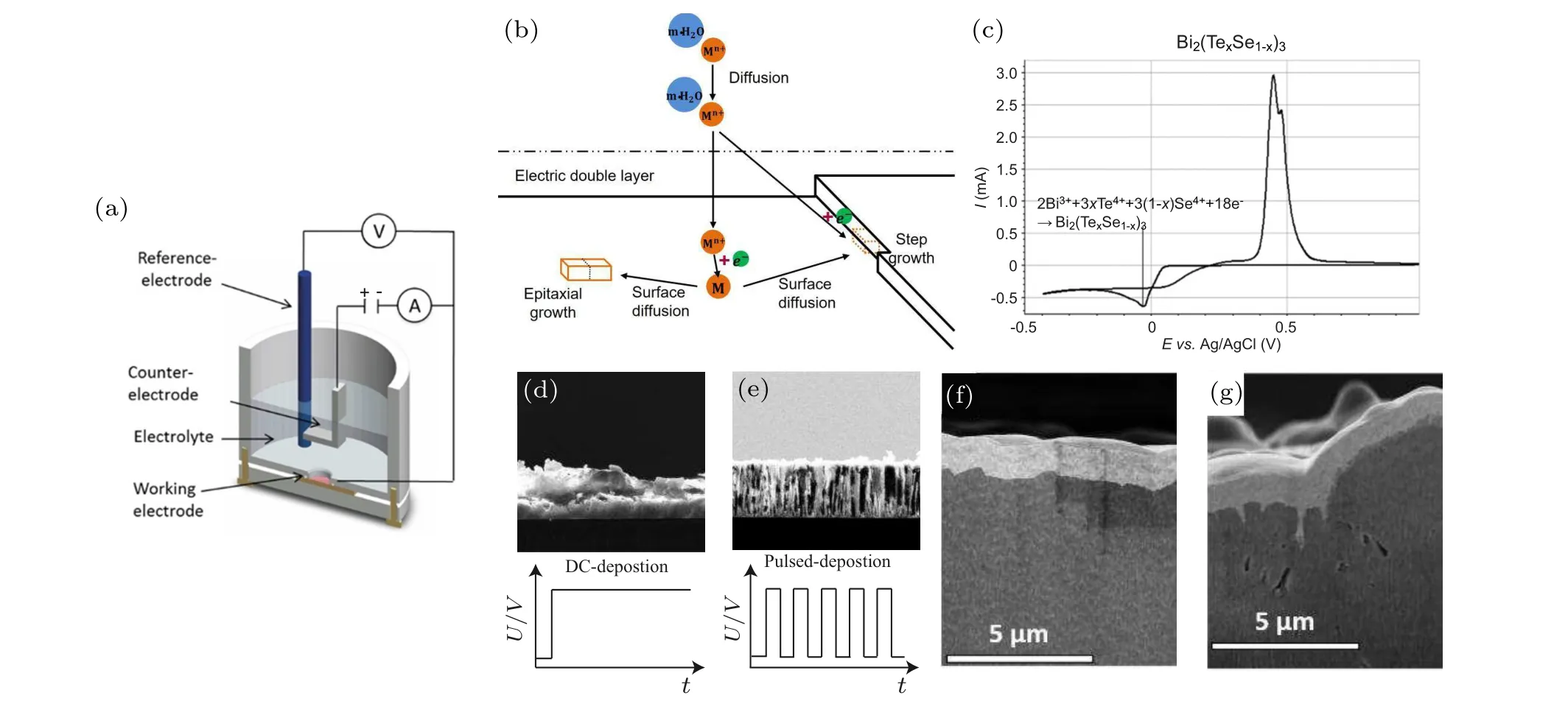
Fig. 3. (a) Schematic setup of electrochemical deposition or measurement. (b) Electrode reaction process of cathodic deposition. (c) Cyclic voltammograms curve of electrolyte containing 0.01 mol/L TeO2,0.01 mol/L Bi(NO3)3·5H2O,and 0.0011 mol/L SeO2 in 1 M nitric acid,the scan speed of 20 mV/s. Reproduced with permission from Ref.[51]. (d)and(e)SEM images of electrodeposits of P-type Sb2Te3 film. Fabricated by constant direct current and pules potential,respectively. Reproduced with permission from Ref.[52]. (f)and(g)SEM images of the upper electrode of Au plus N-type BiTeSe and P-type pure tellurium,respectively. Reproduced with permission from Ref.[25].
3.2. Device aspect
3.2.1. LIGA process
Standard LIGA (German abbreviation: Lithographie,Galvanoformung, and Abformung) is a sequential process first developed by the Nuclear Research Center of Karlsruhe,which includes three basic steps of photolithography,electroplating, and plastic molding.[53]The characteristics of standard LIGA are that it can process microstructures with high spatial resolution and high aspect ratio in large-scale production. However, this method requires further refinement in order to fabricate the structure of Π-shaped like thermoelectric microdevices. Figures 4(a)-4(f) show a typical µ-TE device process flow based on modified LIGA with an innovative top bridge contact method.[25]Starting with a silicon substrate with a thin insulating layer(such as Si3N4)at the top,the conductive layer (such as Gr/Au) is first coated and constructed using standard lithography and etching process(Fig.4(a)),and then a few microns thick Au layer is grown into the new photoresist template cavities by ECD that used as the bottom contact of the thermoelectric elements(Fig.4(b)). Next,the photoresist template for thermoelectric material is fabricated by lithography,after which the N-type and P-type thermoelectric materials are successively electrodeposited into the template of photoresist cavities by ECD(Figs.4(c)and 4(d)).
In general, how to build a top bridge contact is a critical problem within the whole process of the fabrication ofµ-TE devices. Here, we introduce a facile two-step lithography method that is applied to level the bridge areas and realize the suspended bridge construction. In the first step, photoresist with a thickness of exceeding the thickness of thermoelectric legs around 10µm is added to the entire sample and only the bridge areas are selected with a short flood exposure and development, so that only the top few microns of photoresist are removed. With repeating the above exposure and development process, the correct areas of bridge and surfaces of the thermoelectric legs are obtained. Afterward, a thin conducting seed layer is sputtered on the entire sample. In the second step,the same photoresist is added to the whole sample again with thinner thickness. A second lithography stage is carried out directly on the same bridge areas and these areas are fully developed (Fig. 4(e)). Next, a thicker Au layer is electrodeposited to form the bridges. In the final step, all photoresists are stripped away and only freestanding bridges are kept intact(Fig.4(f)).
The American Jet Power Laboratory(JPL)reported a development of µ-TE devices using the modified LIGA processes in 2003,[54]which consists of 126 pairs N-type and Ptype (Bi, Sb)2Te3thermoelectric pillars with 20 µm tall and 60 µm in diameter. The average temperature drop was 2 K at the optimal applied current of 110 mA and the maximum power output was about 1µW,corresponding to a power density of 40µW/cm2with average resistance of 0.26 Ω per couple(Figs.5(a)-5(c)).
Dongyan Xuet al.report a high power density cross-plane µ-TE generator fabricated with microfabrication processes.[55]The TEG contains 127 N-type Bi2Te3and Ptype Sb2Te3thermoelectric elements, demonstrating a maximum power of 2990µW at a temperature difference of 52.5 K and the corresponding power density as high as 9.2 mW/cm2.The power density of this device is the highest value reported for the electrodeposited µ-TEGs in the literature so far. The structure difference between this device and the others is the entire thermoelectric elements are embedded in a permanent SU-8 mold, so that the top surface can be maked extremely even by polished using a rotating textile fabric, which results in the low internal resistance between thermoelectric legs and top connecting metal (Figs. 5(d)-5(f)). Not so long ago,Guodong Liet al. reported an integrated µ-TE cooler with 220 leg pairs (Figs. 5(g)-5(i)), which offers a peak temperature difference of 6 K at around current of 100 mA, a rapid response time of 1 ms, reliability of up to 10 million cycles and cooling stability of more than one month at the constant electric current.[25]This device demonstrates a rarely reported response time, reliability, cooling stability, and high packing density of 5500 leg pairs per cm2and a filling factor of around 20%. The design of freestanding top contacts can reduce the thermomechanical stress in the device,which can take responsibility for high reliability and stability.

Fig.4. The typical process line of theµ-TEDs is fabricated using modified LIGA.Reproduced with permission from Ref.[25].
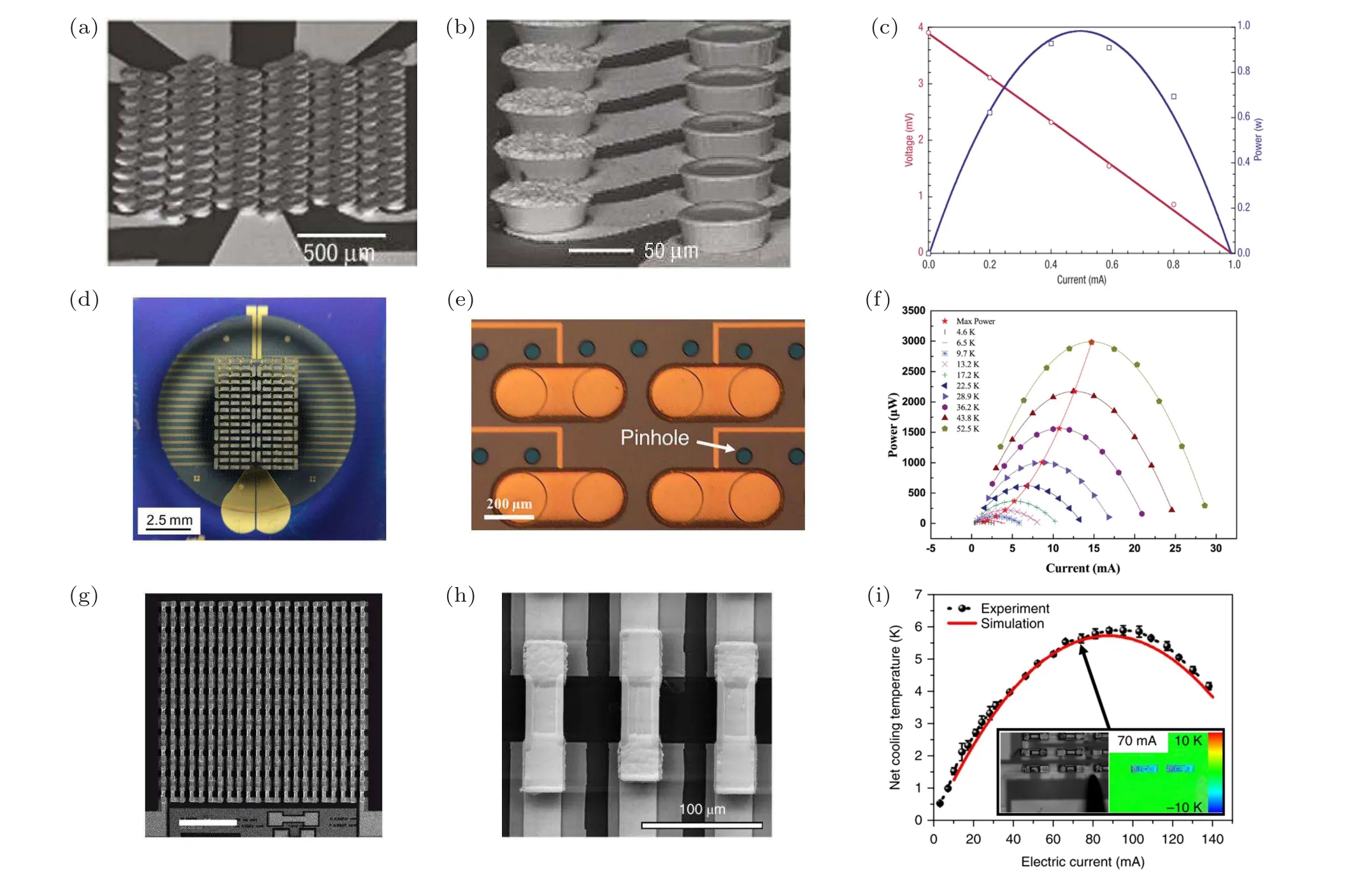
Fig. 5. (a)-(c) The µ-TEDs fabricated by Snyder et al. in 2003. Reproduced with permission from Ref. [54]. (a) Photograph of the completed device.(b)Close-up image of the 40-µm-tall N-type and P-type TE elements.(c)Output voltage power produced by the micro thermoelectric device under the illumination of a lamp. (d)-(f)Theµ-TEG was fabricated by Dongyan Xu et al. in 2016. Reproduced with permission from Ref.[55].(d)Photo of the fabricatedµ-TEG.(e)Close-up image of the diameter of 200-µm pinholes to release thermal stress. (f)The calculated power as a function of current under different temperature differences. (g)-(i)Theµ-TEC was fabricated by Guodong Li et al. in 2018. Reproduced with permission from Ref.[25].(g)Top view of fabricatedµ-TEC.(h)Close-up image of the top view of fabricated thermocouples with the cross-section of 30×40µm2 N-type legs and 30×40µm2 P-type legs. (i)The depression of temperature of fabricatedµ-TEC as a function of applied electric current ranging from 5 mA to 140 mA at the ambient environment of room temperature(~20 °C).
3.2.2. The 3D printing process
The 3D printing, professional named additive manufacturing (AM),[56]is a wide range of manufacturing technologies to create complex 3D objects by utilizing layer-by-layer,line-by-line, or point-by-point deposition methods,[57]which can be used to fabricate thermoelectric materials and construct thermoelectric devices structure.[58,59]Significant progresses have been achieved in high-performance thermoelectric materials based on 3D printing. For example, Xinfeng Tanget al.combined thermal explosion technology with selective laser melting(SLM)for the first time to synthesize high texture Ptype Bi0.4Sb1.6Te3TE material with zTof 1.1 at 316 K,which has both TE properties similar to single crystal and mechanical properties similar to polycrystalline samples.[60]However,in situ3D printing of TE leg or device has not yet been realized in that work.
Direct ink writing of thermoelectrics has also drawn much attention during the past few years because it can fabricate high-performance TE materials and directly construct complex 3D shapes.[61-63]Fredrick Kimet al. fabricated 3D thermoelectric microarchitectures using direct ink writing process,which exhibits high thermoelectric figures of merit of 1.0(Ptype) and 0.5 (N-type), an output voltage of 42.4 mV, and power density of 479.0µW/cm2at a temperature difference of 82.9 K as shown in Fig.6.[64]In their study,chalcogenidometallate(ChaM)was added to fill the voids and change the particle state from molecular ions to crystalline phase to obtain high-quality TE materials after sintering. In addition, by optimizing the particle size,size distribution,and surface states,as-developed all-inorganic TE inks possess higher viscoelasticity and TE performance than others using organic rheological modifiers. Unfortunately, the value of power density does not match the as-achieved zTof materials,and the module has a high resistance of 92 Ω at room temperature, and there is no illustrating of cooling performance,which implies a high interface impedance between the TE legs and Ag electrodes.However,this work shows us a method for manufacturing high-performance µ-TEDs, that is, using direct ink writing to prepare thermoelectric pairs, and exploring new electrode preparation methods to reduce interface resistance(such as ECD).

Fig.6. Theµ-TEDs fabricated by direct 3D writing. Reproduced with permission from Ref.[64]. (a)Illustration of the direct ink writing for 3D architectures. (b)The schematic drawing of the fabrication of theµ-TEDs using direct 3D ink writing. (c)The zT values of printed TE filaments.(d)Output voltage and power of the fabricatedµ-TEG under different temperature differences. (e)Output voltage and power density of theµ-TEG change with temperature difference.
3.2.3. CMOS process
Si-based thermoelectric materials,having various advantages such as low toxicity and production costs,high stability,and large Seebeck coefficients, have drawn increasing attention for µ-TE devices.[65-68]Infineon Technologies reported a µ-TEG based on poly-Si or poly-Si70%Ge30%as the thermoelectric layers.[69]The maximum open circuit voltage of 1 V/K and corresponding electrical output power density of 1µW/cm2have been reported. Aµ-TEG with a heat dissipation path parallel to the thermoelectric layer plane was developed by Xiao Yuet al.[70]The full device consists of 900 pairs of N-type and P-type poly-Si thermocouples,whose maximum open-circuit voltage and the outpower density are 146 mV/K and 0.45 mW/cm2,respectively.The voltage and output power density achieved in the above example are relatively high,resulting from the high packing density and the large temperature differences with the heat dissipation path, which reflect the advantage of CMOS processing to fabricate lateral structurally microdevices and achieve a very high packing density of thermocouples.
With the development of CMOS process technology,the density of thermocouples reaches a very high level, aµ-TEG with a thermocouple number density of 4×106cm-2fabricated by Mark Leeet al. in a recent work[71](Figs.7(a)-7(f)).The TEGs exhibit the maximum output voltage and the record output power density of 4.2 mV and 29 mW/cm2. In this work, the industrial standard 65 nm technology CMOS processing is adopted,and the height of the Si blade has reached 350 nm guaranteeing a not too big internal electric resistance.In particular, under the condition of constant cumulative Si blade cross-sectional gross areas and nearly constant internal electric resistance,the output power increases with decreasing width of the Si blade, which suggests that zTincreases significantly with decreasing width from 240 nm to 80 nm. This result shows that using COMS processing technology to realize nanoscale feature size can not only achieve higher output power density by reducing internal electric resistance but also improve material thermoelectric properties. However,CMOS technology is challenging to realize the series connection of thermoelectric pairs in vertical structure,which offsets the advantage of high packaging density to a certain extent.
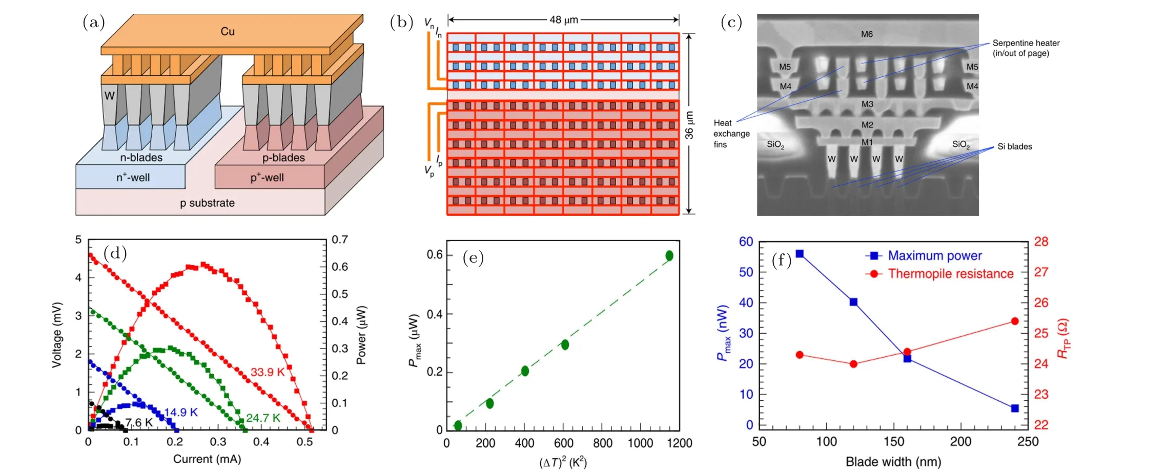
Fig.7. Aµ-TEG fabricated by industrial CMOS process presented by Mark Lee et al. Reproduced with permission from Ref.[71]. (a)Schematical draw of fabricated thermocouples consisting of a group of four N-type and P-type nanoblades and tungsten plugs. (b) Schematic diagram of thermopile plane.The darker blues and darker red rectangles groups are the represents of N-blades and P-blades, respectively. (c) SEM image of a single four-blade TE element with contacts,heat exchange layers and heater. (d)Output voltage and power as function of electric current under different temperature differences.(e) Maximum output power changes with the square of temperature difference. (f) Maximum output power and resistance change with blade width at a temperature difference of 20 K.
3.2.4. Top-down approach
The mechanical properties of the state-of-the-art thermoelectrics based on inorganic semiconductors are generally inferior,[72]resulting in cutting length limit of about 0.3 mm of thermoelectric legs via the traditional mechanical cutting process. Therefore, many efforts based on micromachining technology have been made to miniaturize TE legs.[73-76]For instance, Bottneret al. described a method of regular thinfilm technology combined with microsystem technology in 2004.[77]The fabrication concept is intuitive and easy to understand, as illustrated in Fig. 8(a). First, the N-type Bi2Te3and P-type (Bi, Sb)2Te3thermoelectric legs are manufactured by co-sputtering from 99.995%element targets(Bi,Sb,Te)onto prestructured electrodes on two wafers,respectively.Then the thermoelectric layers are etched by reactive dry etching technique with photoresist as an etching mask. Next,two wafers are welded side by side to form a device. Their followup works have achieved the cooling density of 40 W/cm2and output power density of 11.2 mW/cm2.[78,79]This two-wafer fabrication concept effectively fabricates TEDs with leg sizes ranging from a few microns to tens of microns, however, in some special application areas requiring the size of TE legs to reach 100µm or sub-millimeter,this method becomes hard to achieve or prohibitively expensive.
Jingfeng Liet al. manufactured densely aligned and compact P-N legs by novel silicon molding methods.[80]As shown in Figs. 8(d) and 8(e), they used a silicon mold fabricated by micromachining technology and then filled the molds with molten thermoelectric materials at an air pressure of 1 MPa. This work inspires us with a feasible route to fabricate integratedµ-TEDs,whose thermoelectric pairs thermoelectric performance can be comparable to that of bulk materials.Yuan Denget al. recently reported a zigzag-type thin-film thermoelectric generator assisted by rapid pulse laser patterning technique.[81]In that work,the pulse laser ablation technique is adopted for the first time to pattern the leg arrays,where the electric current flows through the electrodes in a zigzag path.A vertical structure thin film TEG with 200 pairs of TE legs was achieved in a region of 1 cm2, showing an output power density of 1.04 mW/cm2and an open circuit voltage higher than 500 mV at a temperature difference of 88 K. Unfortunately,the cooling performance of the as-fabricated TEDs had not been reported.
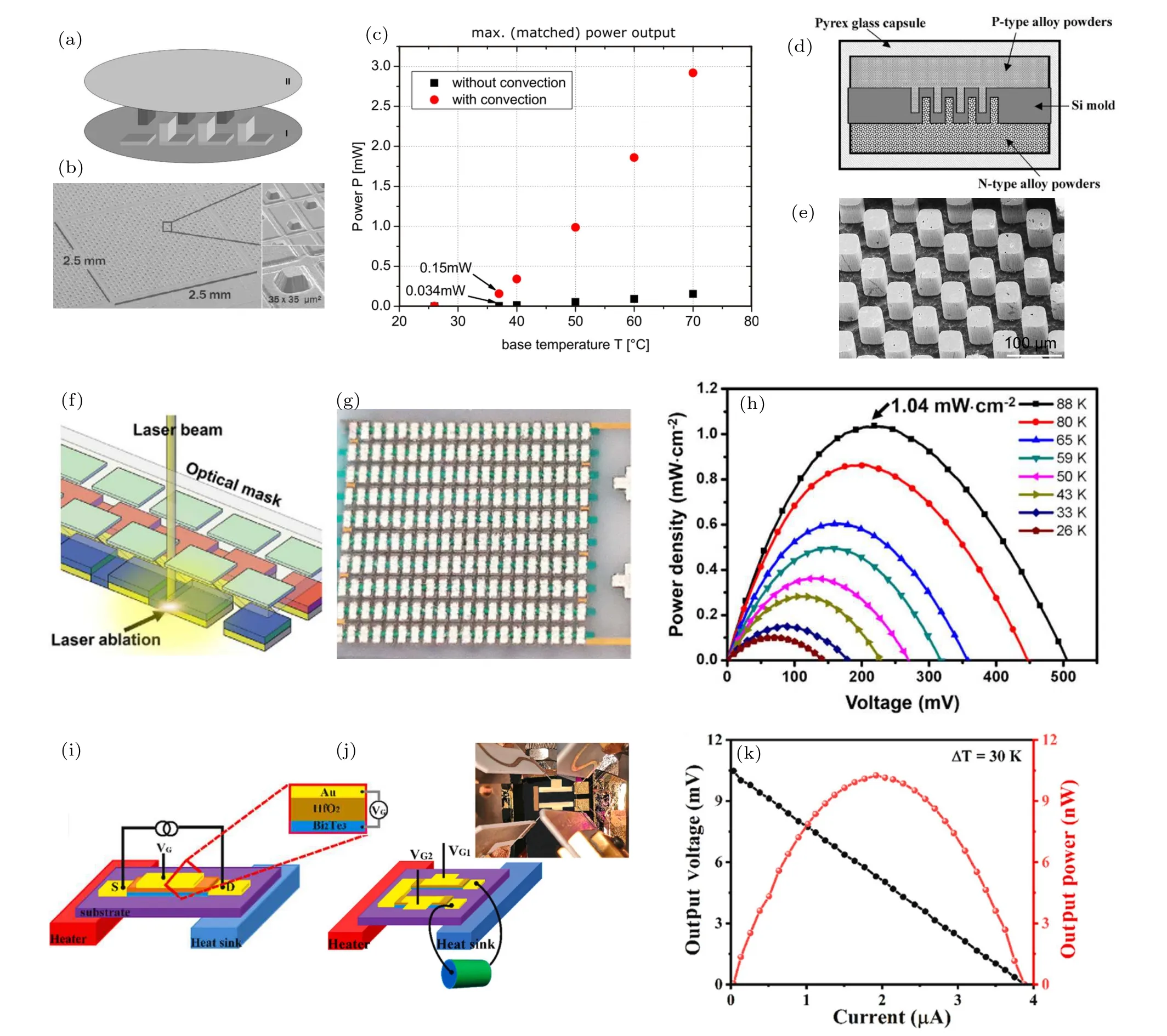
Fig.8. (a)-(c)Two-wafer process to developµ-TEDs presented by Bottner et al. Reproduced with permission from Refs.[77,79]. (a)Illustration of two-wafer concept. (b) SEM image of fabricated µ-TEDs a feature size of ~35 µm square. (c) Output power of fabricated devices under natural convection and forced convection. (d)and(e)Silicon molding process developed by Jingfeng Li et al. Reproduced with permission from Ref.[80]. (d)Schematic drawing of Si mold method. Shape formation of TE legs by squeezing thermoelectric alloy powders into the hole array of Si mold at high temperature. (e)SEM image of developed TE pillars. (f)-(h)Zigzag-type thin-film thermoelectric generator assisted by rapid pulse laser patterning technique presented by Yuan Deng et al. Reproduced with permission from Ref.[81]. (f)Illustration of the process of pulsed laser ablation to pattern the TE materials.(g)Photo of the fabricatedµ-TEG.(h)The output power versus voltage under different temperature differences.(i)-(k) Thin-films thermoelectric devices based on field effect transistor (FET) presented by Yuan Deng et al. Reproduced with permission from Ref.[82]. (i)Schematic draw of the FET structure. (j)Structure of fabricated dual-FET devices;(k)matching output of dual-FET TE devices.
Also, another illuminating work of their team is introduced recently (as shown in Figs. 8(i)-8(k)).[82]Highperformance of thermoelectric materials with the same thermoelectric thin films was achieved by applying different gate voltages on the Te-doped bismuth telluride thin films with intrinsic carrier concentration of 1.05×1017cm3(Ntype). The power factor of the films reached a maximum of 14.9 µW·cm-1·K-2in N-type and 12.5 µW·cm-1·K-2in Ptype under gate voltages of-60 V and-20 V, corresponding to zT >1.22 and zT >1.02 at 303 K, respectively. Under a temperature difference of 30 K near room temperature,the as-fabricated thermocouple can output maximum open circuit voltage and power of 10.5 mV and 10.3 nW,respectively.And interestingly,it can continually adjust the sensitivity from 2.4µV/K to 225.5µV/K by controlling the voltage.This work presented that thermoelectric pairs can be fabricated with the same materials with a simpler and less expensive manufacturing process. However, in authors’own words, “the dual FET structure can be connected in parallel to increase the output current,but how to increase the output voltage in series?” In a word,that work provides a new approach for developing highperformanceµ-TEDs,but there are still challenges in alternatively arranging the N-type and P-type legs.
4. Innovative applications
4.1. IoT and wearable electronics
The Internet-of-Things (IoT) is a fast-evolving field with an expectation of billions of connected devices to the Internet.[83]Sensors are the core of the Internet of Things,which need to be powered by a stable and reliable power supply, ensuring the networked interconnection of the everyday object.[84]At present, the power supply of these devices still mainly depends on chemical batteries.[85]Most microdevices or microsystems are designed to last 15 years or even more,[86]which may pose battery recovery and replacement challenges and raise concerns about potential environmental pollution.There is an urgent need for these devices to operate without external power sources and absorb the energy they need from the environment in which they are placed.
Figures 9(a) and 9(b) show the typical power densities possibly supplied by the home environment and skin temperatures for various body locations,respectively.[87-94]It can be concluded that the domestic environment is the rich source of energy loss ranging from 1.5 µW/cm2to 125 mW/cm2.The measured temperature declines progressively from forehead to feet for the human body under a constant ambient temperature and shows a larger variation under a lower ambient temperature. Due to high thermal resistance between body and ambient air, the heat flow from the skin is about 35 mW/cm2on average.[95]Wireless sensor nodes typically consume about 100 µW of power deployed in the body-area network,[96]which coincides with the power provided by typical thermoelectric generators harvesting energy from human body heat,about 10-30µW/cm2.[97]
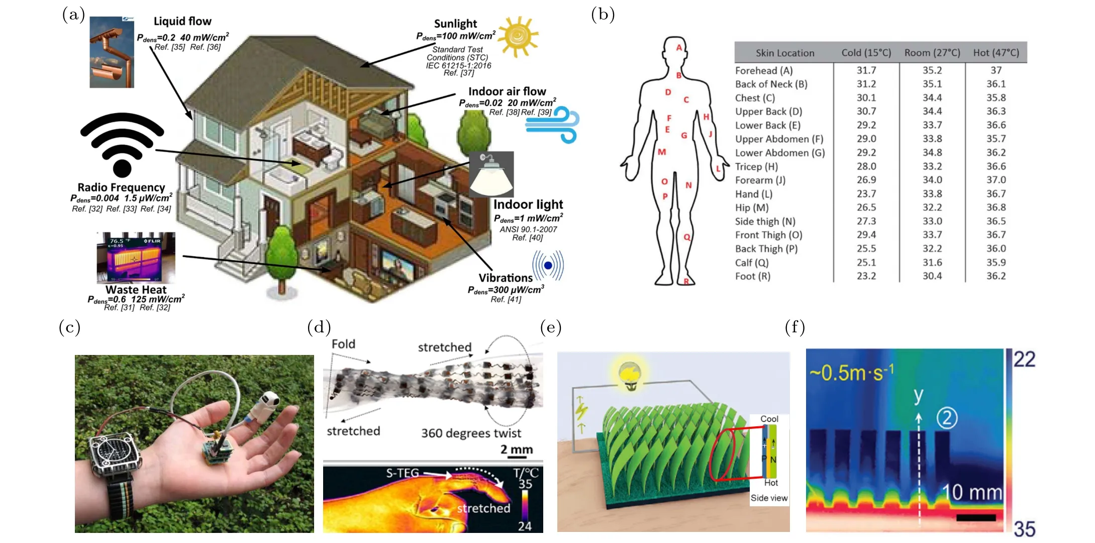
Fig.9. (a)Typical power densities possibly supplied by the domestic environment. Reproduced with permission from Ref.[87]. (b)Evaluation of temperature differences of the human body. Reproduced with permission from Ref.[94]. (c)A watch-like wearable thermoelectric generator with a wireless module and commercial finger pulse oximeter. Reproduced with permission from Ref. [98]. (d) Stretchable thermoelectric generator available for complex and dynamic surfaces. Reproduced with permission from Ref.[99]. (e)-(f)Leaf-inspired flexible thermoelectric generator developed by Weishu Liu et al.Reproduced with permission from Ref.[100].(e)Illustration of leaf-TEG structure and wearable working condition.(f)Temperature distribution profile of leaf-TEG under a testing condition of flowing air rate of 0.5 m/s.
For example, a low-power pulse oximeter fully powered by wearable TEGs was fabricated by Tom TORFSet al. in 2007 as shown in Fig. 9(c).[98]A pulse oximeter is a noninvasive device that indirectly measures the oxygen content in the patient’s blood. Under the condition of measuring every 15 seconds, the average power consumption of the pulse oximeter is only 62 µW, safely within the available 100 µW power that can be provided by the watch-like TEG consisting of 5000 thermocouples. Furthermore, the performance of TEGs has gained continuous improvement in recent years.Yang Yanget al. fabricated a stretchable thermoelectric generator (S-TEG) that can work on complex and dynamic surfaces demonstrating a power density of about 150µW/cm2at ΔT=19 K.[99]The balance between the high performance and flexibility is realized by hot-pressing high-performance P-N elements and the wavy serpentine electrodes(Fig.9(d)).
Many studies focus on how to use environmental heat to generate electricity efficiently. An interesting example is a leaf-inspired flexible thermoelectric generator that makes maximum use of temperature difference ratio recently reported by Weishu Liuet al.[100]In the early morning, we may see a phenomenon: dewdrops are only on the grass leaves rather than evenly scattered on the ground. Such phenomenon results from grass leave that can closely follow the temperature drop of the air with the help of the slender shape and efficient surface heat exchange,while the bottom temperature remains close to the ground.[101]Inspired by the grass leaves,the authors proposed and successfully fabricated a leaf-TEG(Figs. 9(e) and 9(f)), which is made by P-type PEDOT freestanding film, an N-type constantan film, double-sided polyimide tape acting as an electrically insulating layer and Ag paste acting as an electrode(inset of Fig.9(e)).
Under a condition of indoor temperature of 25°C,air velocity of 0.5 m/s,and the substrate temperature at 36°C close to human skin temperature, 10-leaf-TEG (with 10 identical TE leaves,L= 20 mm) possesses a temperature difference across the TE-leaf about 9.35 K, corresponding to a temperature difference utilization ratio of 85%. The temperature difference utilization ratio,φth, firstly proposed by the authors,is defined as the ratio of the ΔTTEGand the available temperature difference(ΔT)between the heat sink and heat reservoir,i.e.,φth=ΔTTEG/ΔT. For comparison, the measuredφthof a commercial TEG module is only 9% under the same condition. Decreasing the length means decreasing the internal resistance so as to improve the output power. The optimized 10-leaf-TEG with TE-leaf lengthLof 10 mm shows aφthof 73% andPmaxof 0.38 µW per leaf under a condition of substrate:36°C,air:6°C,and air flowing:1 m/s.This work gives an inspired answer to the question:How to generate electricity efficiently with limited temperature difference and convection heat transfer conditions?
4.2. Thermally integrated silicon photonics
Integrated silicon photonics has emerged as a suitable photonic platform for large-scale photonic integrated circuits (PICs) for data transmission applications such as optical interconnects, optical switches, and wavelength De/multiplexers.[102-106]However, the performance of such applications using optical components is limited by poor thermal management. For example,the high thermo-optic coefficient,dn/dT,of silicon is 1.8×10⁻⁴K-1that makes refractivity of Si-based waveguide susceptible to temperature fluctuation resulting in the tuning of wavelength filters and spectrum shifting.[107,108]On the other hand, forming a thick low refractive index buried oxide(BOX)layer in the SOI substrate is necessary to achieve low leakage.[109]However,the low thermal conductivity of SiO2will affect heat dissipation, which hinders the improvement of energy efficiency and integration density.[109,110]Figure 10(c) shows a typical schematic representation of a laser array within a PIC package for thermal management. The core thermal aspect is to use macro-TEC overall cooling and locally adjust the temperature of the laser using a resistive heater. The heat load used to adjust the laser temperature will eventually be emitted into the air through air cooling, which undoubtedly increases the full-scale TEC burden and consumes more electrical power to achieve the required laser operating temperature.
An attractive design of thermally integrated chip photonics was presented by R. Enrightet al.[111]As shown in Fig. 10(d), it illustrates the architecture of the thermoelectric temperature controller and its integration conceptually into an integrated photonics system. In that work, the team mainly developed a numerical model to study an integrated design of the micro thermoelectric temperature controller enfolding the waveguide. The results showed that the integrated thermoelectric temperature control is expected to meet the thermal requirements of integrated silicon photonics under the actual operating conditions. Javier Garciaet al. fabricated integratedµ-TEC by template-assisted electrochemical deposition, and the process aims to integrate the cooling device directly on a photoelectronic integrated circuit (PIC).[112]As shown in Figs. 10(e) and 10(f), the cross-section of a single leg and the gap between the legs are 20×100µm2and 8µm, which matches the size of the waveguide.Unfortunately,the finite element simulation results show an enormous contribution of the contacts to the overall electrical resistance,which is increased by the roughness of the Bi2(TexSe1-x)3and (BixSb1-x)2Te3top surface.
4.3. Microfluidic with local temperature controlled
Microfluidic chip, also called lab-on-the-chip, is a technology to control the microliter or nanoliter liquid in the micrometer channel structure,[116-118]which can flexibly combine multiple unit technologies in the system to form a network structure to achieve chip-scale integration,shorten sample processing time,significantly improve measurement resolution and sensitivity, thus greatly reducing consumption and cost.[119]Microfluidic chip technology has been widely used in clinical testing,[120]point of care,[121]micro reaction and flow chemistry,[122]cell growth,[123]high throughput drug screening,[124]and other fields. According to the data statistics from Yole analysts in 2019,[125]the global market size of microfluidic products reached 8.7 billion US dollars in 2018,with a compound annual growth rate of 11.7%between 2019 and 2024, and it is expected to reach 17.4 billion US dollars in 2024. Being integrated with active cooling and heating technologies, microfluidics has been able to exploit fundamental properties of cryobiology, such as the relationships between cell membrane permeabilities,[126]cell division,[127]cell metabolism,[128]etc. and temperature. Traditionally, the lab on chip with temperature distribution is constructed by overall cooling and local heating as shown in Fig.11(c).

Fig. 10. (a) Schematic drawing of a tunable laser. Reproduced with permission from Ref. [113]. (b) The thermo-optic coefficient of silicon and fused silica versus temperature. Reproduced with permission from Ref. [114]. (c) Schematic drawing of the traditional thermal of photonic integrated circuit package solution with TE devices.[115] (d) Conceptual diagram of integrated photonics system with µ-TED. Reproduced with permission from Ref.[111]. (e)and(f)Aµ-TEC integrated with a photonic circuit fabricated by Javier Garcia et al. Reproduced with permission from Ref.[112]. (e)Schematic picture of theµ-TEC integrated with a photonic circuit. (f)Close-up of a part of the fabricatedµ-TEC.
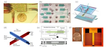
Fig. 11. (a) Photo of a microfluidic chemostat. Reproduced with permission from Ref. [117]. (b) Photo of a simple, inexpensive microfluidic diagnostic device. Reproduced with permission from Ref. [117]. (c) Schematic 3D structure of a temperature controllable microfluidic device.Reproduced with permission from Ref.[126]. (d)Conceptual diagram of the integrated microchannel with aµ-TEC.Reproduced with permission from Ref. [131]. (e) Schematic diagram of a thermoelectric microfluidic sensor. Reproduced with permission from Ref. [132]. (f) A thin-film thermoelectric device fabricated on polyimide support that may integrate with the microfluidic chip. Reproduced with permission from Ref.[133].
For example,Dayong Gaoet al. fabricated a microfluidic platform that combines a local temperature heater and a widerange coolants bath to achieve large-scale accurate temperature control.[129]Through simulation analysis, the integrated microfluidic platform has large-scale temperature control in the range between 2°C and 37°C.[130]Zeling Leiet al. created a similar microfluidic chip using water bath and microheater to overall cooling and local heating, and they used the platform to investigate simultaneously the osmotic behavior of multiple oocytes.[126]
Obviously,strategy as mentioned above has achieved success in realizing broad range temperature control at a specific site. However, only local low temperature cannot be implemented. The µ-TECs are active cooling devices with small feature size and could direct integration with the chip seemed likely to solve the problem. Gary Rosengartenet al.demonstrated a concept of aµ-TEC integrated into a microfluidic channel with rapid and local fluid cooling (as shown in Fig. 11(d)) and developed an analytical thermal model to analyze the key parameters to achieve the reasonable cooling efficacy.[131]For it to be realized,a key aspect is that a second embedded microfluidic channel needs to be used as a miniature heat sink.Besides,the performance of the cooler is highly determined by the thermal resistance between the hot and cold connections,the quantity of fluid,as well as the thermal conductivity of substrates. It is expected to achieve a temperature drop of about 1 K by using common parameters, while the prototype devices show a temperature difference of 2±1.5 K with a current of 0.7 A.Its outcomes are less than ideal. However,it is worth mentioning that the height of the usedµ-TECs is 200µm,which means the cooling density has the potential to increase 10 times if the height of the device decreases to 20µm.
Beyond the above applications based on Peltier effect,thermopile-based sensors integrated with a microfluidic chip,work on Seebeck effect. By monitoring the outputting DC voltages,one can measure the biological or chemical heat energy inside the microfluidic chip to determine the direction and extent of the reactions. A thermoelectric microfluidic sensor(TMS)consisted of a 100µm deep microfluidic channel with a Bi/Sb thin film thermopile with a Seebeck coefficient of around 7 µV/mK and excellent rejection of common mode thermal signals was recently described.[132]It can detect a small dynamic temperature change in the order of 10-4K.Based on the structure and design of the device,the team measured the heat released during the hybridization of two complementary single stranded nucleic acids in a series of subsequent experiments,[133]and successfully sequenced a DNA sequence composed of 12 base pairs,which fully confirmed that this technology could be used for the unmarked detection of nucleic acid sequences. The thermoelectric method simplifies the detection of a nucleic acid sequence by eliminating additional enzyme reactions or DNA fluorescence labeling. The team also reported a thermoelectric method for enzyme-linked immunosorbent assay (ELISA) in a microfluidic device.[134]The thermopile was used to measure the heat of the enzyme reaction between glucose and glucose oxidase to determine the concentration of the analyte.The feasibility of the thermoelectric method of chip laboratory ELISA is verified by measuring the concentration of 8-hydroxy-2-deoxyguanosine in the urine of transgenic mice with amyloid precursor protein.
5. Conclusion and perspectives
Undoubtedly, thermoelectric microdevices possess twofold great advantages over full-scale devices. On one hand,microdevices offer high applicability and suitability to integrate with both microscale and macroscale applications such as specific site cooling/heating, energy harvesting, and sensing due to their scalable size and shape. On the other hand,µ-TEDs present a potentially higher output power or cooling density owing to their smaller internal resistance than conventional size devices, which provides a guarantee for generating electricity meeting the requirements of applications under small temperature differences. So far, high-performance thermoelectric thin films and advanced manufacturing technology have achieved great achievements, respectively. Future research directions should focus on how to use integration technology to develop thermoelectric microdevices using high-performance thermoelectric materials while realizing the characteristics of high zT, optimal geometric configuration,and almost negligible contact resistance.
To date,using electrodeposition combined with lithography process can fabricate intimate contact and size-scalable micro thermoelectric devices, however, the as-developed Ptype thermoelectric materials have poor thermoelectric properties due to their irregular and unconsolidated morphology.P-type semiconductors synthesized by cathodic reduction deposition commonly show a dendrite morphology that may result from the fact that the reaction is a minority carrier reaction. This conclusion is supported by the phenomenon of cathodic current at the P-type electrode increased by light excitation. Accordingly, a dense morphology may be obtained by cathodic reduction deposition with laser irradiation. Thus,even if a dense film is formed, enough electrons can be provided to guarantee the reduction reaction performing continuously and effectively. This is worth more research and exploration. Besides that, performance improvement is usually achieved by some post-treatment method. Actually, an optimization of composition, charge carrier density, and mobility for P-type(BixSb1-x)2Te3has been achieved by annealing in different ambient atmospheres.
In the aspects of device design and fabrication,more extensive innovative opportunities emerge from printing,ink direct writing,bionics,multidisciplinary integration,etc.to simplify the machining process and/or enhance the performance of devices. The ability of 3D printing technology provides the opportunities to rapidly fabricate microdevices with desired shapes and integrate them into specific areas. Inspiring from some interesting phenomena in nature,we may generate numerous ideas to function and perform advantages of thermoelectric devices with innovative configuration. High energy laser can quickly melt or even ablate many materials,by which high performance or patterned thermoelectric materials have been successfully fabricated. Moreover,the emerging femtosecond laser technology seems to achieve this goal with high efficiency and high precision.
At present,the researches ofµ-TEDs mainly focus on the development of high-performance devices, and some innovative applications ofµ-TEDs are in their infancy. The high performance ofµ-TEDs is the key and foundation for large-scale applications. However, mature products are usually achieved through continuous iterative optimization. Hence, it is very necessary to develop applications with as-fabricated µ-TEDs to consistently generate high-quality thermoelectric products.The future success of realizing the wider impact of µ-TEDs depends on the leap in the performance of thermoelectric materials,advanced device design and manufacturing,and innovative applications.
Acknowledgments
The authors acknowledge the funding support of the National Key Research and Development Program of China(Grant No. 2018YFA0702100)and the National Natural Science Foundation of China (Grant No. 52172259). We thank Jiawei Yang and Nan Chen for valuable discussions.
猜你喜欢
小天使·一年级语数英综合(2022年4期)2022-04-28
儿童时代(2022年4期)2022-04-19
国际太空(2022年1期)2022-03-09
军事文摘(2021年22期)2022-01-18
小哥白尼(军事科学)(2020年10期)2021-01-18
百科探秘·航空航天(2020年10期)2020-10-27
学苑创造·A版(2019年8期)2019-08-15
军事文摘·科学少年(2017年4期)2017-06-20
军事文摘·科学少年(2017年1期)2017-04-26
军事文摘·科学少年(2017年1期)2017-04-26

- Chinese Physics B的其它文章
- Quantum walk search algorithm for multi-objective searching with iteration auto-controlling on hypercube
- Protecting geometric quantum discord via partially collapsing measurements of two qubits in multiple bosonic reservoirs
- Manipulating vortices in F =2 Bose-Einstein condensates through magnetic field and spin-orbit coupling
- Beating standard quantum limit via two-axis magnetic susceptibility measurement
- Neural-mechanism-driven image block encryption algorithm incorporating a hyperchaotic system and cloud model
- Anti-function solution of uniaxial anisotropic Stoner-Wohlfarth model