
Research status and performance optimization of medium-temperature thermoelectric material SnTe
2022-04-12 03:47PanPanPeng彭盼盼ChaoWang王超LanWeiLi李岚伟ShuYaoLi李淑瑶andYanQunChen陈艳群
Chinese Physics B 2022年4期
关键词:王超
Pan-Pan Peng(彭盼盼), Chao Wang(王超), Lan-Wei Li(李岚伟), Shu-Yao Li(李淑瑶), and Yan-Qun Chen(陈艳群)
Institute for Computational Materials Science,School of Physics and Electronics,Henan University,Kaifeng 475004,China
Keywords: SnTe,thermoelectric materials,electronic transport,thermal conductivity
1. Introduction
Energy production and conversion is one of the most important activities of any society. Fossil fuels-coal, oil, and natural gas-currently play a significant role in fulfilling the global energy demand and will still remain the primary sources of energy in driving economic growth through 2040.[1]For example,almost 90%of the electricity supply relies on fossil fuels in 2010.[2]However,fossil fuel is a non-renewable energy source and 70%of the energy of fuel combustion is wasted in the form of heat by the engine or factory system, discharged together with exhaust gas (500-800 K) or taken away by the cooling system.[3]Therefore,there exists strong environmental and economic pressure to increase the thermal efficiency of fossil fuel by utilizing the waste heat energy. Thermoelectric materials can directly convert between heat and electricity without any emission or vibration components,providing an opportunity to obtain useful electricity from waste heat in cars, factories, and other energy-intensive processes.[4]At present, thermoelectric materials have already been used in many fields, such as thermal power plant, automotive industry, solar thermal systems, implantable or wearable devices,and deep-space probes.[3]
Currently, the biggest challenge that limits the wide applications of thermoelectric materials is the low conversion efficiency. The performance of thermoelectric materials can be assessed by the dimensionless figure of meritZT,defined as the lattice thermal conductivityκl, and the bipolar thermal conductivityκbipolar.[5]From the definition ofZT, it can be clearly seen thatZTcan be improved by increasing Seebeck coefficient and electrical conductivity, and reducing thermal conductivity. However, these parameters have a strong coupling relationship and are all related to the carrier concentration through the following relationship:[6]

Here,kB,q,h,m∗,µ, andLare the Boltzmann constant,the carrier charge, the Planck’s constant, the effective carrier mass, the carrier mobility, and the Lorentz number, respectively. The interdependent relations of the thermoelectric parameters are intuitively shown in Fig. 1.[7]It can be concluded from Fig. 1 that changing one parameter to improveZTvalue is hardly implemented. So far, there have been many strategies developed to weaken the coupling relationship between the parameters. Modulation doping[8,9]and band enginering[10,11]can effectively enhance carrier mobilityµ, so higher electrical conductivityσis obtained accompanying with smaller decrease of Seebeck coefficient. Additionally, energy filtering effect,[12,13]resonant levels,[14]ionization scattering[15]and band convergence[16,17]can effectively improve Seebeck coefficient by increasing the energy dependence ofµ(E)or increasing the density of states near the Fermi level. From Fig. 1, it can be found that lattice thermal conductivityκLis an independent parameter,which is conve-
whereSis the Seebeck coefficient,σthe electrical conductivity,Tthe absolute temperature, andκthe total thermal conductivity including the electronic thermal conductivityκe,nient to reduce by enhancing phonon scattering. So far,point defects,[18-21]dislocations,[22,23]grain boundaries[24,25]and nanoparticles/nanoprecipitates[12,26]have already been used to enhance phonon scattering and successfully reduced the thermal conductivity of thermoelectric materials. Attributed to the above strategies,remarkable advances have been made recently in obtaining high-performance thermoelectric materials.

Table 1. A summary of the thermoelectric performance of SnTe-based thermoelectric materials in recent years.
As one of the best medium temperature thermoelectric materials,lead telluride(PbTe)has already reached relatively highZT(>2.0).[61-64]However,its practical application in a wide range is limited by the toxicity of Pb. Since Sn and Pb are in the same main group and SnTe has the similar crystal and band structure with PbTe,SnTe has attracted great interest as a substitute for PbTe. However, the thermoelectric performance of SnTe is not as good as that of PbTe, mainly due to the following reasons:[65-67]1) a smaller and direct band gap(0.18 eV at 300 K)leading to a strong bipolar effect;2)a large energy separation between the light valence band and the heavy valence band (0.3 eV and 0.15 eV at 300 K for SnTe and PbTe, respectively), this makes the heavy hole valence band basically not participate in the electron transport,consequently resulting in lower Seebeck coefficient;3)a large number of inherent Sn vacancies in SnTe leading to the excessive carrier concentration (1020-1021cm-3), resulting in higher electronic thermal conductivity and poor Seebeck coefficient; 4) the smaller atomic mass of Sn compared to Pb,leading to the higher lattice thermal conductivity. Researchers have adopted a variety of strategies to overcome those shortcomings of SnTe to improve its thermoelectric properties. The over high carrier concentration can be modulated by doping and self-compensation.Energy band engineerings,such as valence band convergence and resonance energy level, are innovative ways and used to increase the Seebeck coefficient.Meanwhile,nano-engineering and other novel micro-structure design and full-scale structure are used to reduce the thermal conductivity. Figure 2 shows the timeline of the maximumZTfor SnTe-based thermoelectric. From Fig. 2, we can clearly observe that the thermoelectric performance of SnTe is enhanced step by step and some significant progress has been made based on the mentioned strategies. In Table 1, the typical results of SnTe are summarized and presented in detail.However,although researchers have tried their best to improveZTof SnTe,it still can not compare with that of PbTe. Therefore,further improving the SnTe-based thermoelectric performance is current main goal. In this review, we introduce the recent development of SnTe and summarize the key strategies for SnTe performance optimization, and then propose the future development direction of improving SnTe thermoelectric performance. It is hoped that this will inspire and guide researchers for future development of SnTe-based thermoelectric materials.

Fig.1. Schematic diagram shows the dependence of Seebeck coefficient S,electrical conductivity σ, thermal conductivity κ and power factor S2σ on carrier concentration n. Reproduced with permission from Ref.[7]. Copyright 1968,Elsevier.

Fig.2. The timeline of the maximum ZT values for SnTe-based thermoelectric materials. Data are from Refs.[12,16,27,29-36,38-60,66,68-83].
2. Crystal structure and band structure
As mentioned above,most shortcomings of SnTe as thermoelectric materials originate from its band structure, while band structure is mainly determined by the crystal structure of material. SnTe has three crystal structures: rhombohedral structure (α-SnTe), rock-salt structure (β-SnTe) and orthorhombic structure (γ-SnTe).[84]α-SnTe is a low temperature phase and can only exist stably at a temperature lower than 100 K.γ-SnTe is its high pressure phase and can be transformed fromβ-SnTe at 18 kbar.[85]Generally,SnTe used as thermoelectric material isβ-SnTe, which has cubic structure with space groupFm¯3mand the lattice parameters ofa=6.3268 °A andα=90°.[84]The crystal structure ofβ-SnTe is shown in Fig.3(a). Whenβ-SnTe is twisted along the direction of[111],it can transform into rhombohedralα-SnTe. For example,local rhombohedral structural distortions can appear inβ-SnTe by heavily doping Ge, which shows significant effect on thermal conductivity.[86]Local structural distortion ofβ-SnTe was also observed by Maet al.using neutron powder diffraction at 625 K.[16]So, the structure transformation betweenαandβphases presents an efficient strategy to modulate the thermal conductivity of SnTe.
Figure 3(b) shows the band structure of SnTe calculated using density functional theory(DFT)with the spin-orbit coupling (SOC) effect.[16]It can be clearly seen that SnTe has a direct band gap and the valence band maximum (VBM)and conduction band minimum (CBM) are both located atLpoint. The band gap is about 0.108 eV, which is consistent with other calculation results(0.11[87,88]and 0.12 eV[89])and smaller than the values measured by photoluminescence experiment (0.18 eV[90]). Additionally, according to the theoretical results, the band gap can be significantly decreased with the concentration of Sn vacancies increasing (0.02 eV for Sn0.96Te).[16]When the Sn vacancy concentration is high,the defect energy level has merged with the continuum to form a large band tail, which leads to the effective band-gap narrowing.[91]This phenomenon has been confirmed by other theoretical results.[87]The too small band gap is unfavorable to the enhancement of thermoelectric performance due to the bipolar effect. It can also find that the maximum of the heavy hole valence band is located atΣpoint (betweenΓandKpoints).The energy separation between the light and heavy valence bands,ΔEL-Σ,is about 0.254 eV.Rogers pointed out that the light and heavy hole valence bands are nonparabolic and parabolic,respectively,[92]which is confirmed in Fig.3(b). In order to more intuitively observe the symmetry and degeneracy of the band,the high-symmetrykpoint and the isoenergy surface atE=-0.38 eV in the first Brillouin zone of SnTe are shown in Fig.3(c). VBMLlies at the center of the(111)Brillouin zone face and has 8 half-pockets,so its valley degeneracy is 4. The valley degeneracy ofΣpoint is 12. Usually,the holes are confined to highly anisotropic and nonparabolic pockets.[93]Once the energy shifts downward by 0.38 eV from the Fermi level,the hole pockets would interconnect with theΣband and merge to an open network of tubes,which means that bothLandΣbands contribute to carrier transport.In other words, once the heavy hole valence participates in the carrier transport,the number of degenerated valleys will increase from 4 to 16, which is desirable for increasing the Seebeck coefficient.
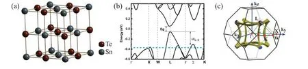
Fig.3. (a)The crystal structure of β-SnTe. (b)Energy band structure with SOC for SnTe. (c)The first Brillouin zone of SnTe and the isoenergy surface at E=-0.38 eV.Panels(b)and(c)adapted with permission from Ref.[16]. Copyright 2019 American Chemical Society.
3. Optimization strategies
At first,almost all thermoelectric materials were obtained through countless attempts and personal experience. The scientific basis of thermoelectric materials was well established in the 1950s.[94]So far,based on continually developing thermoelectric theory, researchers have already developed systemic strategies to optimize the performance of thermoelectric materials.[95]For the enhancement of the electrical properties,adjustment of carrier concentration,modulation doping,band engineering (valence band convergence, resonance energy level) and energy filtering are used. As for the thermal performance,since the lattice thermal conductivity is an independent parameter, lots of work focus on the decrease of the lattice thermal conductivity. Point defects, dislocation, grain boundaries,nanoparticles,and nano-precipitates have all been proven to effectively enhance phonon scattering and decrease the lattice thermal conductivity. Additionally, the synergy of multiple strategies shows better results on the improvement of the thermoelectric properties. Here,we will review the effect of these strategies on SnTe-based thermoelectric materials from the point of view of electrical and thermal properties respectively.
3.1. Optimizing carrier concentration
As shown in Fig. 1, the Seebeck coefficient, electrical conductivity, and electronic thermal conductivity are closely interrelated with each other through the carrier concentration.Therefore, optimizing carrier concentration has turned to be a key strategy in achieving a highZTvalue. Generally, the optimal carrier concentration for most thermoelectric materials is in the range of 1019cm-3to 1021cm-3. However,this optimal value is variable and strongly depends on the properties of the material itself and temperature. Specifically, the optimal carrier concentration is proportional to (m∗dT)1.5under the assumption of single band conduction and the approximation of classical statistics,wherem∗dis the density of state effective mass.[96]The strong dependence of the optimal carrier concentration on temperature has further led to the need for a higher carrier concentration in a given material to reach the optimalZTvalue of the material at high temperatures.[97]This can guide us to determine the optimal carrier concentration according to the expected application temperature of different materials. Using a three-band model (CB, VBLand VBΣ),Honget al.calculated that the optimal carrier concentration of SnTe corresponding to the maximumZTvalue is 2×1020cm-3at 800 K.[98]Theoretical results obtained by Tanet al.indicated that the optimizedZTvalue of Mn doped SnTe at 800 K and Cd doped SnTe at 750 K can be reached at 2×1020cm-3and 1.5×1020cm-3,respectively.[87]At room temperature,the optimal carrier concentration of SnTe is about 1×1018cm-3.[99]
However, pristine SnTe is always p-type with high hole concentration(1020-1021cm-3)at room temperature induced by intrinsic high vacancy concentration.[122]Huoet al.studied the defects in SnTe by using the density functional theory(DFT)[100]and the calculation results are shown in Fig. 4(a).It can be seen that Sn vacancy (V2-Sn) has the lowest defect formation energy under either Sn-rich or Te-rich condition.Especially in the case of the Sn-poor condition,Sn vacancy is easily formed because the formation energy is always negative. While,under the Sn-rich condition,the formation energy of VSn2-is partly above 0 in the band gap range, which suggests that the hole concentration will be restricted by the doping limit of the Sn vacancies. The Sn-rich condition can be realized through off-stoichiometry strategies. Tanet al.investigated the effects of Sn self-compensation on the reduction of the hole carrier concentration.[83]The limit for Sn-compensation in SnTe is 0.03 and the hole concentration reduces from 4.7×1020cm-3(pristine SnTe)to 2×1020cm-3(Sn1.03Te).Due to the optimizing hole concentration,Sn1.03Te has aZTvalue of~0.6 at 823 K,which is 50%improvement over the pristine SnTe. It should be mentioned that the hole concentration shows almost no change when the concentration of self-compensation Sn exceeds 0.03. Therefore,another effective approach to tune carrier concentration,extrinsic doping, should be used. Naturally, aliovalent elements from the neighboring columns of the periodic table that serve as the donor dopants are the first choice to decrease the hole concentration. As shown in Fig. 4(b), Sb, Bi, Mn and In are the most common elements acting as donors in SnTe. Especially, the carrier concentration of most of Bi doped SnTe is on the order of 1019cm-3and Sn0.97Bi0.03Te shows the highestZTvalue of~0.9 at 880 K.[49]Additionally,I doping by
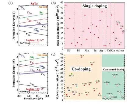
Fig. 4. (a) Calculated defect formation energy of SnTe as a function of the Fermi level under Sn-rich and Sn-poor conditions. Reproduced with permission from Ref. [100]. Copyright 2021, Royal Society of Chemistry. Carrier concentration of SnTe obtained by (b) single doping, (c)co-doping and compound doping. The data come from Ref.[14,27,38,48,49,53,56-58,60,65,68,72,76,78,79,81-83,89,99,101-121]
substituting Te of SnTe can significantly reduce the carrier concentration to 3.01×1019cm-3.[110]Isovalent doping of Cd, Pb, Mg, Ca elements can also decrease the carrier concentration because of the decreasing vacancy concentration.[58,82,83,111]Except for single doping,co-doping and compound doping are often used to adjust the hole concentration. Co-doping is a promising strategy that can simultaneously tune the hole concentration and realize resonance energy level or valence band convergence.For example,by co-doping Bi and In,a significant enhancement on the thermoelectric performance with a peakZTof 1.26 at 900 K was achieved.[49]It can be observed from Fig.4(c)that one of the commonly used co-doping elements is In.Theoretical and experimental results suggest that In element is able to introduce the resonant level in SnTe.[14,107]Additionally, compound doping can also tune the carrier concentration because the elements of compound will diffuse in SnTe matrix during the preparation process and reduce the Sn vacancy concentration. Maet al.reduced the carrier concentration of Sn1.03Te to 3.01×1019cm-3by doping MgAgSb.[20]BiCl3compound has been employed to dope into SnTe and the maximumZTof~1.27 at 873 K has been obtained in the sample of SnTe doping with 4%BiCl3,which enhances by 182%in comparison with the pristine sample.[65]
3.2. Band engineering
The power factor of the material is mainly determined by the energy band structure,so adjusting the energy band structure can optimize the electrical properties of the thermoelectric material. The main methods of band engineering for thermoelectric materials include: 1) increasing the carrier effective mass; 2) the generation of the resonance energy level; 3) valence band convergence.
3.2.1. Increasing carrier effective mass
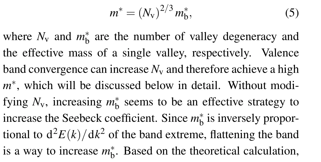
It can be seen from Eq.(2)that Seebeck coefficient is directly proportional to the effective mass of carriersm∗. So increasingm∗is an effective way to increaseS.m∗can be determined by the following equation:[123]

3.2.2. Resonance energy level
In 1950, Korringa and Gerritsen first proposed the concept of resonance doping. In some cases, the energy level of the dopant that locates in the conduction band or the valence band leads to a distortion of the host band, which is called a resonant state.[124]The resonance state introducing by doping can significantly enhance the Seebeck coefficient by the strong distortion of energy-related DOS and resonance scattering. Equation(2)shows that the Seebeck coefficient depends on the carrier density in per unit energy interval near Fermi energy (dn(E)/ndE).n(E) is defined asn(E)=g(E)f(E).Here,g(E) is the density of states (DOS) andf(E) is the Fermi function. Therefore, increase or sharp features of the DOS nearEFwould lead to a high Seebeck coefficient.[6]The resonant state can generate a hump in the DOS, as shown in Fig.5(a).When the Fermi level moves close to the hump,g(E)is significantly increased and therefore the Seebeck coefficient is enhanced. Additionally, the energy dependent relaxation time in the presence of resonant scattering can be described with the formula[125]

whereEis the carrier energy level,EDis the resonance energy level, andΓis the resonance horizontal width. Carriers with energy equal toEDare strongly scattered by resonance scattering,resulting in an increase inS.[125]However,at room temperature and above, the effect of resonance scattering onSis often weak. So the main effect of resonance doping is increasing the DOS near the Fermi energy level.

Fig. 5. (a) Schematic diagram of the influence of resonance energy level on density of states. (b) The Seebeck coefficients at room temperature for different material systems with obvious resonance effect. (c) The schematic diagrams of the band structure for impurity doping SnTe at low temperature and high temperature. Panels(b)and(c)reproduced with permission from Ref.[37]. Copyright 2020,Elsevier.
In recent years,many thermoelectric materials have been applied to this strategy, such as Sn doped Bi2Te3[126]and Tl doped PbTe.[6]As for SnTe,the most commonly used element to generate resonance energy levels is In.[16,66,127]In Fig.5(b),it can be clearly seen that the Seebeck coefficients of In doped SnTe obvious deviate from the solid line,the Pisarenko curve,which means the occurrence of resonance effect. Zhanget al.found that theZTvalue of In0.0025Sn0.9975Te at 873 K reached 1.1, which was about three times higher than that of the pristine SnTe sample.[14]According to theoretical calculations, the DOS near the Fermi level is significantly higher than that of the original SnTe, indicating that In doping in SnTe leads to a resonance state.[107]In 2019,Bhat and Shenoy reported that Zn also can be a resonant dopant in SnTe using first-principles density functional theory calculations.[128]This conclusion was further confirmed by experimentalZTof~1.49 at 840 K for Zn doped SnTe. Although the resonance effect has been widely used,it is still difficult to predict resonance dopants. To clarify the mechanism of resonant dopants and to simply uncover resonant dopants,Yanget al.used density functional theory to clarify the mechanism of resonant dopants and provided a simple method to discover resonant dopants. They predicted that a variety of elements (including Y, Ru, In, Sb, La, Gd, Lu, Os, Tl and Bi) can be used as resonance dopants for SnTe. It should be noted that the resonant doping effect will fail at high temperature. Electrical transport is usually provided by the carriers near the Fermi surface,and the resonance energy level determined by the impurity level needs to be located near the Fermi level,as shown in Fig.5(c). High temperature usually changes the position of impurity level and Fermi level and leads to the failure of increase of Seebeck. For SnTe, when the temperature is above 600 K,resonant doping effect is weak and unable to increase theZTvalue.[37]
3.2.3. Valence band convergence
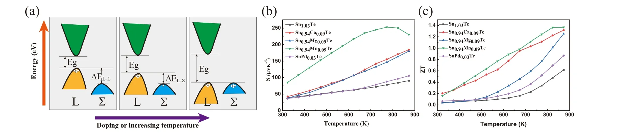
Fig.6. (a)Schematic diagram of band convergence of SnTe. (b)Seebeck coefficient and(c)ZT value as functions of temperature for pristine SnTe and Mn,Ca,Mg,Pd doped SnTe. The data come from Refs.[16,51,58,82].
As shown in Fig. 6(a), valence band convergence is to reduce the energy separation between the heavy hole valence band and the light hole valence band through chemical doping, so that the heavy holes participate in the electrical transport,thereby increasing the number of carrier transport channels and improving the electrical transport characteristics.[123]From Eqs.(2)and(5),it can be known that using the method of valence band convergence to increaseSis to increase theNv. IncreasingNvallows heavy holes to participate in the carrier transport andm∗increases without affectingµ. Generally,Nvcan be increased by proper doping and increasing the temperature. About the effects of temperature on band convergence, the power factor increases when ΔEL-Σbecomes smaller at high temperature and it shows the highest value when the temperature is 900 K(ΔEL-Σ=0,the light valence band and heavy valence band totally converge).[98]Selecting appropriate dopant can also reduce ΔEL-Σ, for example, Ag,Ca, Hg, Mg, Mn, Pd and Sr.[16,47,51,58,82,89,129]For Ca doped SnTe, ΔEL-Σdecreases from 0.42 to 0.2 while theZTvalue increases from 0.4 at 900 K to 1.35 at 873 K for the pristine SnTe and the Sn0.94Ca0.09Te,respectively.[58]As for Ag doping in SnTe,ΔEL-Σis reduced to 0.186,and theZTvalue is increased to 1.35 at 900 K.[129]The thermoelectric performance is improved by more than 100% due to Ag doping.[129]To compare the effects of different dopants on the valence band convergence, the Seebeck coefficient andZTvalue as functions of temperature for pristine SnTe and Mn, Ca, Mg, Pd doped SnTe are shown in Fig. 6(b) and 6(c). It can be seen that the maximum Seebeck coefficient of Mn doped SnTe can reach 254 µV·K-1. TheZTvalue of Mn doped SnTe is also the largest comparing with other samples, reaching 1.35 at 873 K, which is more than 100% higher than 0.62 at 873 K for pristine SnTe. Therefore,Mn element as the dopant shows the better effect on the valence band convergence.
3.3. Energy filtering
The calculation results show that the carriers which have higher energy between 0.05 eV and 0.1 eV contribute the most for high Seebeck coefficient and low-energy carriers actually reduce the Seebeck coefficient.[130]Therefore, by introducing potential barriers using dispersed nanostructures in bulk materials, lower-energy carriers can be filtered and the average carrier energy can be increased(namely,energy filtering),which will lead to the Seebeck coefficient increase.Figure 7(a)shows the schematic diagram for energy filtering effect induced by additional secondary phase. When the size of the second phase (λ) is reduced to~10 nm, the quantum confinement effect appears. This quantum confinement effect will form a band gap lower than VBM in the p-type semiconductor,and then only filter out low-energy holes.[95]Energy filtering effect can be also inferred from Eq.(2)that the Seebeck coefficient can be enhanced by increasing the energy dependence of the carrier mobility (dµ(E)/dE). The concept of energy filtering in thermoelectrics was first proposed by Ioffe and further developed by Rowe and Min.[131,132]Energy filtering can only slightly reduce the electrical conductivity while the Seebeck coefficient is enhanced, so the power factor increases.Many experimental results confirmed that energy filtering effect can effectively enhance the thermoelectric performance.For example, Zhouet al.doped SnTe with ZnO to produce energy filtering effect by bending the energy band, and theZTvalue reached 0.9 at 873 K.[133]Comparing with a single barrier,multiple barriers can further enhance the energy filtering effect. Maet al.introduced BiCuSeO@SnO2core-shell nanostructures into the SnTe matrix by doping the BiCuSeO nano-alloy and multiple potential barriers can be fromed,[12]as shown in Fig. 7(b). BiCuSeO@SnO2core-shell nanostructures result in a heterogeneous interface between the SnTe matrix and the shell, the interface between the shell and the core, and the layers within the core. BiCuSeO@SnO2coreshell nanostructures can significantly improve the Hall mobility and obviously reduce the carrier concentration compared with other doped nano-alloys.[20,54,60,78]It can be observed from Fig.7(c)that the carrier concentration could decrease to about 10%while the mobility is increased to 350%compared to the value of the undoped sample at room temperature when the BiCuSeO doping concentration is over 3%.
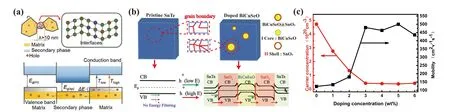
Fig.7. (a)Schematic diagram for energy filtering effect of additional secondary phase due to quantum confinement effect. Reproduced with permission from Ref.[95],Copyright 2020 Wiley Publishing. (b)Schematic diagram of doped BiCuSeO@SnO2 core-shell nanostructures introducing multiple potential barriers in SnTe. (c) The carrier concentration and mobility of Sn1.03Te-x%BiCuSeO at room temperature. Reproduced from Ref.[12]with permission from the Royal Society of Chemistry.
3.4. Reduce thermal conductivity
In a solid,the interaction between atoms produces a displacement from their equilibrium positions, resulting in a series of vibration waves of different wavelengths,the so-called phonons.[94]In addition to improving electrical performance,reducing thermal conductivity through the scattering of various phonon can also optimize the thermoelectric performance of the material. As we all know, the thermal conductivityκis composed of three termsκe,κLandκb.κbarises as a consequence of electron-hole pair creation at the hot side and recombination at the cold side. In the case of degeneracy,only minority carriers affect bipolar thermal conductivityκb.[134]In order to suppress the bipolar thermal conductivity,it is necessary to reduce the minority carrier transport, which can be achieved by enlarging the band gap. SnTe has a bipolar thermal conductivity due to a band gap of only 0.18 eV.[90]Doping and alloying are the commonly adopted strategies to manipulate the bandgap,which are usually related to the optimization of electron transport. There is a similar situation forκe,which links withσvia the Wiedemann-Franz law. So,here we only discuss the reduction of the independent parameterκL.

Fig. 8. (a) Schematic diagram of the relationship between phonon scattering rate and frequency of different mechanisms.[136] Reproduced under the terms of the CC-BY Creative Commons Attribution 4.0 International License (http://creativecommons.org/licenses/by/4.0/). Copyright 2016, The Authors, published by Springer Nature. (b) Schematic diagram illustrating various phonon scattering mechanisms within a thermoelectric material,along with electronic transport of hot and cold electrons. Reproduced with permission from Ref.[139],Copyright 2010 Wiley Publishing.
The lattice thermal conductivityκLis determined by the specific heat capacityC, the phonon group velocityυsand the phonon relaxation timeτq. These parameters are all related to the phonon frequency, especially the relaxation time of the phonon.[135,136]As we all know, phonon waves can be scattered by introducing various types of crystal defects(such as point defects,[112]dislocations,[22]interfaces,[137]and precipitates[25,138]). Figure 8 presents the schematic diagram of the frequency-dependent phonon scattering rates for various mechanisms. Point defects are particularly effective in scattering high frequency phonons (Rayleigh scattering), while nano-inclusions are the main scattering mechanism for low-frequency(long wavelength)phonons,and grain boundary scattering plays a major role for short wavelength phonons.[136]
3.4.1. Point defect scattering
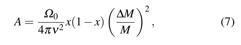
In the thermoelectric material, point defects may be the native point defects (vacancies) or extrinsic point defects induced by doping elements(substitutional or interstitial atoms).All the point defects inevitably lead to the the fluctuations of mass and strain field,which can reduce the lattice thermal conductivity by scattering high frequency phonons, as shown in Fig.9(a).The scattering factor can be evaluated by the following equation:[140]
whereΩ0,ν,x, ΔM,Mare the volume of the unit cell, the lattice sound velocity, the fraction of guest atom, the atomic mass difference between the guest and the host,and the average mass of the cell,respectively. Therefore,to maximize the degree of reduction of lattice thermal conductivity, the doping atoms and the host atoms should have the larger atomic mass (ΔM). When the point defect is the vacancy, the value of ΔM/Mis maximized at a value of unity. In other words,the vacancies have the maximal high frequency phonons scattering. Tanet al.found that AgSbTe2alloying could increase the cation vacancy concentration in SnTe from 0.7%to 4.6%. It can be observed from Fig.9(b)thatκLdecreased from 0.7 W·m-1·K-1at room temperature to 0.4 W·m-1·K-1at 800 K attributing to the increase of Sn vacancy,[54]which was close to the amorphous limit of SnTe. SnTe alloying with other compounds, such as In2Te3, NaSbTe2, AgBiTe2, also shows similar results,as shown in Fig.9(c).
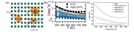
Fig. 9. (a) Schematic diagram of phonon scattering at strain fields induced by point defects including vacancies, substitutional and interstitial atoms. (b) Lattice thermal conductivity modeling under Debye approximation. The further reduction from gray to blue (blue shaded region) is due to increased[VSn]and phonon-vacancy scattering. Reproduced with permission from Ref.[54]. Copyright 2018 American Chemical Society.(c)Lattice thermal conductivity of In2Te3,AgSbTe2,NaSnTe2,AgBiTe2 doped SnTe. The data come from Ref.[54,60,80,121].
3.4.2. Nanoprecipitate
The phonons with medium and long wavelengths may be strongly scattered by nanoprecipitate with feature sizes comparable to their wavelengths. Therefore, the introduction of nanoprecipitate or nanoinclusions into bulk materials can significantly reduce the lattice thermal conductivity. Generally,a relatively low volume fraction of the second phase (usually a few mole percentage) is the best choice to achieve the strongest phonon scattering. At higher volume fractions,nanostructures can aggregate or combine into larger structures with a lower interface area,thereby weakening their scattering efficiency.[94,141,142]The size of these nanostructures is larger than the mean free path of electrons or holes, phonons are more likely to be scattered by the interface without blocking the transport of electrons.[130]While maintaining the carrier mobility and electronic conductivity,the thermal conductivity of the lattice is effectively reduced. By doping 3% MgAgSb into SnTe during the preparation, Maet al.observed using SEM and TEM that MgAgSb nanoparticles formed in the matrix and the diameters varied from several nanometers (second phase) to several micrometers. MgAgSb nanoparticles could strongly scatter phonon and consequently make a significantκLreduction at medium temperature,which could be seen from Fig.10(c).

Fig.10. (a)and(b)SEM and HRTEM images of MgAgSb doped Sn1.03Te sample,respectively. (c)Lattice thermal conductivity as the function of temperature for MgAgSb doped Sn1.03Te sample. Reproduced with permission from Ref.[20],Copyright 2019 American Chemical Society.
The consistent embedding and complete alignment of the guest component and the host matrix is called endotaxial nanostructuring,[46]as shown in Fig. 11(a). These structures can effectively inhibit the heat flow in the system using the acoustic mismatch between the components but do not affect the carrier mobility.[137]Hussainet al.introduced the endotaxial Cu2Te nanostructures into SnTe,[46]which plays a dominant role in reducing the lattice thermal conductivity. In Fig.11(b),high density moir´e fringes can be found around the nanoprecipitates, which is due to the interference of two sets of crystal planes with nearly similar periodicity and/or small relative rotation angle. The lattice image of moir´e fringes in Fig. 11(c) indicates Cu2Te nanoprecipitates are endotaxially placed in the SnTe matrix. Figure 11(d) shows that doping different materials in SnTe to form endotaxial nanostructuring reduces the lattice thermal conductivity. At 873 K, the lattice thermal conductivity of doping Cu2Te nanoparticlesis is significantly reduced to~0.27 W·m-1·K-1,which is even smaller than the minimum thermal conductivity calculated by Debye-Cahill theory. However, under the modified Bornvon Karman periodic boundary condition,the amorphous limit of SnTe is expected to be as low as~0.12 W·m-1·K-1.[144]Therefore, the experimental lattice thermal conductivity can still be reasonable. Due to the ultra-low thermal conductivity, a highZTvalue of 1.5 at 873 K is achieved by introducing endotaxial Cu2Te nanostructures into Ge and Sb codoped SnTe.[145]When Sb is doped to form the composition Sn0.85Sb0.15Te,κLdrops to 0.67 W·m-1·K-1at near room temperature. Doping SrTe into Sn0.97Bi0.03Te can also form the second phase. At 823 K, the lattice thermal conductivity decreases from 1.5 W·m-1·K-1of the pure phase to 0.8 W·m-1·K-1,and theZTvalue reaches 1.2.[103]
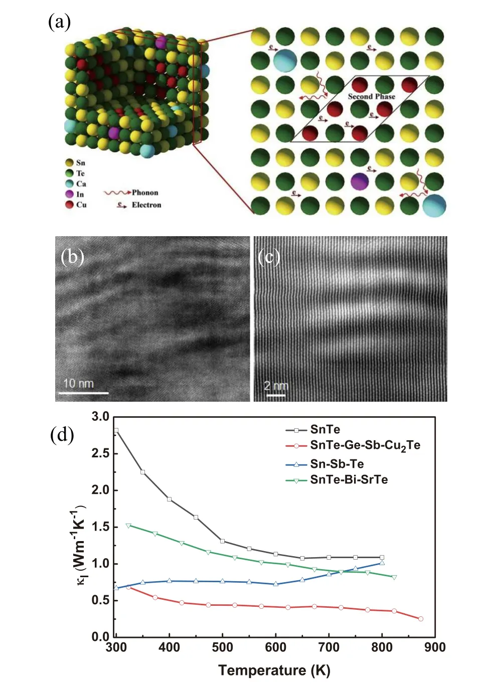
Fig. 11. (a) Schematic diagram of endotaxial nanostructuring in SnTe system. (b) HRTEM image shows plenty of disperse moir´e fringes;(c) atomic resolution HAADF-STEM image of moir´e fringes around the nanoprecipitates. Panles(a)-(c)reproduced with permission from Ref.[46],Copyright 2020, Elsevier. (d) Lattice thermal conductivity of SnTe,Sn0.92Ge0.04Sb0.04Te-5%Cu2Te,Sn0.85Sb0.15Te,Sn0.97Bi0.03Te-SrTe. The data come from Refs.[103,104,145].
3.4.3. Mesoscale structure
The scattering rate of phonons is closely related to the mean free path of phonons (MFP). The phonons of MFP<1 nm can be scattered by atomic-scale point defects,and those with MFP of 1-10 nm and 10-1000 nm can be scattered by nano-precipitates and mesoscale crystals.[94]In order to further reduce the lattice thermal conductivity, it is necessary to introduce crystal defects and structural features in the micron and sub-micron length range to scatter the mid-wavelength and long-wavelength phonons. Typically,the sizes of grains in the single crystals are>10 µm, while the materials with grain size from 0.1 µm to 3 µm are called mesoscale crystals.[94]Roweet al.proved that the large-sized crystal grains are not effective in reducing the thermal conductivity,while the crystal grains with feature size less than 5 µm can strongly scatter the phonons.[24]Kihoiet al.found that mesoscale grain boundary can be form in SnTe by doped Mn, Bi, and Sb.[73]With the introduction of mesoscale grain boundary coordinated point defects and nano-precipitation in the crystal, its lattice thermal conductivity decreases to 0.86 W·m-1·K-1at 873 K, and theZTvalue reaches 1. Similarly, Zhanget al.obtained Ag0.11Gd0.06Sn0.94Te by codoping Gd and Ag into SnTe.[77]The introduction of mesoscale scattering of grain boundaries and nano-precipitates in the crystal reduced the lattice thermal conductivity to 0.6 W·m-1·K-1at 873 K.Except for doping,there are other methods to obtain mesoscale grains:grinding the coarse crystals into fine powder by ball milling,mechanical alloying, melt spinning or self-propagation hightemperature synthesis.[146-149]Comparing with doping, the mesoscale grains size can be easily controlled by these means,which are the most commonly used ways to reduce the lattice thermal conductivity.
4. Summary and outlook
SnTe has attracted great interest as a promising medium temperature thermoelectric material. The theoretical calculation suggests that theZTvalue of SnTe can reach up to 2.2.[98]Currently, theZTvalue does not meet the researchers’ expectations and it is still necessary to devote efforts to further improve its thermoelectric properties to promote its commercial application. Many advanced technologies have been applied to improve the electrical properties of SnTe,such as valence band convergence, resonance energy level and energy filtering. Meanwhile,to reduce the lattice thermal conductivity, point defects, nanoprecipitates, and mesoscale structures are used to effectively maximize phonon scattering. Recently,arising from the synergy of the multiple strategies, SnTe has made great progress and a peakZTcan reach 1.85. Although tremendous progress has been made in SnTe,more fundamental research is still needed to enhance its electrical and thermal properties and makes it a suitable candidate for the actual application.
As mentioned above,the optimal carrier concentration is proportional to(m∗dT)1.5,which means that it depends strongly on temperature. Generally, the optimal carrier concentration in SnTe at room temperature may be achieved by the Sn selfcompensation or doping. However, precisely controlling the optimal carrier concentration under different temperatures is still a big challenge because the Sn vacancy concentration,the concentration of ionized impurities and the band gap vary with the temperature. Additionally, it is worth to further explore whether the optimal carrier concentration can be maintained after several thermal cycles.In terms of thermal properties, although the lattice thermal conductivity can be reduced to 0.4-0.5 W·m-1·K-1through multiple scales of defects at high temperature, it is still far above the amorphous limit of SnTe(0.12 W·m-1·K-1)predicted by Chenet al.[144]Therefore,new strategy should be developed to further decrease the lattice thermal conductivity of SnTe.
As for the real application of SnTe, the lack of n-type SnTe is one obstacle to develop thermoelectric module because the stable module requires both n- and p-type thermoelectric materials with similar physical and chemical properties. SnTe almost always exists in the p-type due to the high concentration of Sn vacancies. Moshwanet al.pointed out that the n-type study of SnTe is an opportunity and a challenge.[143]The theoretical calculation suggests that the Seebeck coefficient of n-type SnTe is even superior to that of n-type PbTe.[152]Modern strategies such as controlled highefficient cation-anion codoping can produce n-type materials.In fact, there is little research about n-type SnTe. In 2021,n-type SnTe thermoelectric materials with remarkable performance were successfully synthesized through suppressing Sn vacancies,followed by electron-doping.[153]In detail,through Pb alloying and I doping,the n-type Sn0.6Pb0.4Te0.98I0.02can achieve a notably highZTmax~0.8 at 573 K. However, this work involves Pb element. N-type SnTe without Pb is probably the next big challenge in this field.
It is well known that the mechanical strength is an important factor for thermoelectric module production. The thermoelectric materials should be strong enough to withstand thermal cycling, thermal shock and machining. For SnTe, Sn vacancies will reduce the mechanical strength.[154]SnTe exhibits highZTat relatively high temperatures (800-950 K). Therefore,mechanical properties will deteriorate due to the increasing Sn vacancies when SnTe shows best thermoelectric performance at high temperature. Additionally,Muthumariet al.confirmed that SnTe is brittle in nature based on density functional theory.[155]Appropriate dopants or alloying,leading to fewer Sn vacancies and crack growth suppression,can increase the rigidity of SnTe.[154,156,157]However,the mechanical properties of SnTe still need to be further improved for thermoelectric devices and more detailed work should be carried out.
All in all, in order to improve the thermoelectric performance of SnTe, further efforts are needed. We hope that this review can spark broad interest and provide insights and new strategies. We also expect a revolutionary breakthrough in SnTe in the near future.
Acknowledgment
This research was sponsored by the National Natural Science Foundation of China(Grant Nos.U1504511,11674083,and 12005194).
猜你喜欢
电影文学(2022年16期)2022-09-26
中国应急管理科学(2022年2期)2022-05-23
中国应急管理科学(2022年2期)2022-05-23
中国应急管理科学(2022年1期)2022-04-18
广告大观(2019年8期)2019-09-10
娃娃乐园·3-7岁综合智能(2017年8期)2018-02-01
娃娃乐园·3-7岁综合智能(2017年8期)2018-02-01
娃娃乐园·3-7岁综合智能(2016年6期)2016-09-19
三月三(2016年3期)2016-03-23
广西教育·D版(2015年5期)2015-06-16
- Chinese Physics B的其它文章
- Quantum walk search algorithm for multi-objective searching with iteration auto-controlling on hypercube
- Protecting geometric quantum discord via partially collapsing measurements of two qubits in multiple bosonic reservoirs
- Manipulating vortices in F =2 Bose-Einstein condensates through magnetic field and spin-orbit coupling
- Beating standard quantum limit via two-axis magnetic susceptibility measurement
- Neural-mechanism-driven image block encryption algorithm incorporating a hyperchaotic system and cloud model
- Anti-function solution of uniaxial anisotropic Stoner-Wohlfarth model