
Laser-induced phase conversion of n-type SnSe2 to p-type SnSe
2022-04-12 03:47QiZheng郑琦RongYang杨蓉KangWu吴康XiaoLin林晓ShixuanDu杜世萱ChengminShen申承民LihongBao鲍丽宏andHongJunGao高鸿钧
Chinese Physics B 2022年4期
Qi Zheng(郑琦) Rong Yang(杨蓉) Kang Wu(吴康) Xiao Lin(林晓) Shixuan Du(杜世萱)Chengmin Shen(申承民) Lihong Bao(鲍丽宏) and Hong-Jun Gao(高鸿钧)
1Beijing National Center for Condensed Matter Physics and Institute of Physics,Chinese Academy of Sciences,Beijing 100190,China
2School of Physical Sciences,University of Chinese Academy of Sciences,Beijing 100190,China
3CAS Center for Excellence in Topological Quantum Computation,University of Chinese Academy of Sciences,Beijing 100190,China
4Songshan Lake Materials Laboratory,Dongguan 523808,China
Keywords: SnSe2,SnSe,laser irradiation,local phase conversion
1. Introduction
In the past years, transition metal dichalcogenides (TMDs) have attracted intensive research interests due to their diverse electronic properties, such as metal/band insulators,[1-3]semiconductors,[3-7]charge density waves,[8-10]ferromagnetism,[11]valley polarization,[12,13]etc. These versatile properties come from the diversity of their compositions and phases, including trigonal prismatic(2H), octahedral (1T), rhombohedral (3R), monoclinic (1T')phases,[14,15]etc. Due to the weak bonding energies in metalselenium bonds,there is a low energy requirement to lose Se in selenide minerals and the phase transition in selenide minerals is widely reported.[16-18]Recently, an electron-beam induced phase conversion technique has been reported in which the electrons accelerated up to 300 keV in a transmission electron microscope (TEM) system gain enough energy for knocking a weak bonded atom(for example Se in PdSe2)[19]out of the sample and thein-situTEM observation provides the possibility of understanding the phase conversion mechanism in atomic scale. Besides the mechanism study, this local phase transition technique also provides high controllability to form semiconductor homojunction when the two phases before and after conversion have different properties,such as by converting n-type to p-type semiconductor, a p-n junction can be fabricated. Compared with the traditional nanomicro fabrication to prepare semiconductor p-n junctions by locally ion implantation, the local phase conversion technique is more efficient and has better controllability.
For the tin selenides, stable layered crystal phases(Fig. 1(a)) are known with Sn in Sn(IV) [SnSe2, n-type] and Sn(II) [SnSe, p-type] oxidation states. The p-n junction of SnSe2and SnSe formed by local phase conversion of n-type SnSe2to p-type SnSe within-situelectron beam irradiation in a TEM was firstly reported by P.Shutteret al. in 2016.[16]After that,thermally driven conversion of n-type SnSe2to p-type SnSe by direct heating is developed and in-plane p-n junction has been formed.[20]Creating in-plane p-n junctions at predefined locations is critical for further exploration of the novel properties and device applications of SnSe2-SnSe heterostructure. Here,we report laser-induced transformations of layered tin dichalcogenides from n-type SnSe2to SnSe. By collecting Raman spectra on SnSe2flakes before and after laser irradiation, the phase conversion from n-type SnSe2to p-type SnSe is confirmed. The conversion mechanism of laser heating effect induced removal of Se atoms from SnSe2is revealed by the Raman spectra collected at different substrate temperatures and laser power levels. Lattice resolved transmission electron microscope (TEM) images confirms such conversion at atomic levels. Finally, a pattern with SnSe2/SnSe heteostructures is created by selective laser irradiation on SnSe2flakes,indicating that the laser induced phase conversion technique has relatively high spatial resolution and enables the creation of micron-sized in-plane p-n junction at predefined region.
2. Methods
2.1. Growth of SnSe2 nanoflakes
The SnSe2nanoflakes were grown by chemical vapor deposition (CVD) on a mica substrate using Se and SnI2pills as precursors,[21]as schematically shown in Fig. 1(a). The substrate was loaded into a double heating zone CVD furnace and placed 20 cm down steam to a quartz crucible containing 13.5 mg of SnI2(≥99.999%, Alfa) with another quartz crucible containing 400 mg of Se(≥99.999%,Alfa)in the upper steam. The Se pills in the first heating zone were heated up to 470°C in advance to insure a Se rich environment. Then the SnI2pills were heated up to 530°C in 10 min and kept for 15 min under a flow of 5 sccm H2+20 sccm Ar carry gas. The key step to get thin and large SnSe2nanoflakes is fast cooling down the substrate to room temperature after the growth progress.
2.2. Sample characterization and laser irradiation progress
Optical microscope(BX51,OLMPUS)and atomic force microscope (SPA 400, SII) in tapping mode were used for characterization of the morphology and thickness of SnSe2flakes. TEM images and SAED pattern were taken by JEOL JEM-2100 at an accelerating voltage of 200 kV.TEM samples were prepared by directly scraping SnSe2flakes from the as grown substrate and collecting them on TEM grid. Laser irradiation on SnSe2flakes was performed by the laser in a confocal Raman/PL system(Horiba HR-Evolution)and the Raman spectra were collectedin-situbefore and after the phase conversion process. A home updated variable temperature(VT)-VACUUM Raman system (Horiba HR-800) was used for the temperature dependent conversion.
3. Results and discussion
3.1. Synthesis and characteristic of SnSe2 nano flakes
The SnSe2flakes were synthesized by a CVD method.[21]Figures 1(b) and 1(d) show the optical micrograph of the asgrown SnSe2flakes. The SnSe2flakes show either hexagonal or triangular shapes, which can be controlled by varying the substrate temperature. As shown in Fig. 1(c), the lateral size of the triangular shaped flake can reach up to~80 µm.Its thickness was measured by line profile analysis of atomic force microscope(AFM).An AFM image of the SnSe2flake is shown in the inset of Fig.1(c)and its thickness is measured as~2.1 nm. The lateral size of hexagonal SnSe2nano-flake can reach up to~30µm(Fig.1(e)). High-resolution transmission electron microscopy (HRTEM) was used to characterize the lattice structures of the SnSe2nanoflakes. The lattice fringes shown in Fig. 1(f) indicate a perfect atomic structure with a lattice spacing of 3.3 °A, corresponding to the (10¯1) planes of a hexagonal-phase SnSe2.[22]Further selected area electron diffraction(SAED)pattern also confirms the high quality and single-crystalline nature of SnSe2,as shown in the inset of Fig.1(f). The element analysis of Sn and Se by energy dispersive x-ray spectroscopy(EDX)study shows a 1:2 atomic ratio of Sn versus Se,as shown in Fig.S1. The Raman spectrum in Fig. 1(g) shows clear peaks of the Egmode at 117 cm-1and A1gmode at 185 cm-1,respectively,which is consistent with previous result.[23]
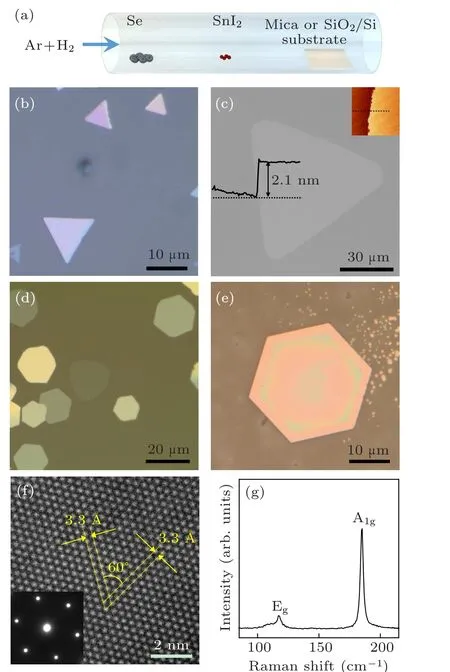
Fig. 1. Preparation and characterization of single crystalline SnSe2 flakes.(a)Schematic diagram of the preparation of SnSe2 flakes by CVD.(b)Optical image of triangular SnSe2 flakes as-grown on a mica substrate. (c)Optical image of an individual SnSe2 flake with thickness of 2.1 nm. Inset is the AFM image of the same SnSe2 flake. (d)Optical image of hexagonal SnSe2 flakes as-grown on a mica substrate. (e) Optical image of an individual SnSe2 flake with hexagonal morphology. (f) Lattice-resolved TEM image of a single SnSe2 nanoflake.Inset is the SAED image.(g)The Raman spectrum collected on a typical SnSe2 nanoflake.
3.2. Laser induced conversion from SnSe2 to SnSe
In Raman spectrum measurements, the Raman scatter signal increases with the gain of laser power and if high laser power is applied, the sample may be burnt by heating effect.Figure 2(a)shows the burnt holes at top corner and right corner of a triangle SnSe2nanoflake after collecting Raman spectrum for 60 s with laser power of 25 mW under a 532 nm laser irradiation. To study the laser irradiation effect on the structure of SnSe2flake,Raman spectra were collected before and after the laser irradiation process. As shown in Fig.2(b),the black line and red line represent the Raman signals before and after the laser irradiation progress, respectively, and the blue lines show the peaks fitting after the laser irradiation.In comparison to the Raman signal from SnSe2, new Raman peaks located at 69 cm-1, 93 cm-1and 153 cm-1emerge after the laser irradiation, which represents the A1g, B3gand A3gvibration modes of SnSe crystal,[24]respectively. This indicates that by laser irradiation on SnSe2flake, SnSe2can be converted to SnSe. In addition,the A1gpeak at 185 cm-1and the Egpeak at 117 cm-1of SnSe2remain after the laser irradiation,which indicates that SnSe2is not completely converted to SnSe. This is because that during laser irradiation the heat distribution of the irradiation area is not uniform. Figure 2(c)shows a simple sketch of the laser irradiation progress. The core part has a higher temperature than the edge of the outer area,so the conversion from SnSe2to SnSe may happen only in the core part.An AFM image of the burnt hole is shown in the upper inset of Fig.2(c),which initially confirms that the laser heating effect might be the physical mechanism of the conversion. Furthermore, an area conversion progress is performed by point-bypoint laser irradiation on SnSe2flake, as shown in Fig. 2(a).Figure 2(d)shows the Raman spectra collected from the area of original SnSe2(black),after point conversion(red)and after area conversion(blue),respectively. The green dashed rectangle highlights that the A1gpeak of SnSe2located at 185 cm-1is substantially reduced after area conversion, indicating that the SnSe2is almost completely converted to SnSe.
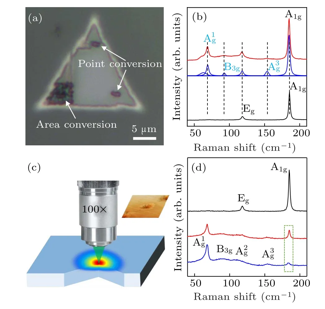
Fig. 2. Laser induced phase conversion of n-type SnSe2 to p-type SnSe.(a)Optical microscope image of the SnSe2 flake with point conversion and area conversion. (b)The Raman spectra before(black)and after(red)conversion together with peak fitting(blue). (c)The schematic diagram of the heat distribution during conversion and the 3D AFM image of a burnt hole(upper inset). (d)Raman spectra of original SnSe2 (black),after point conversion(red)and area conversion(blue),respectively.
3.3. The temperature-and laser power-dependent conversion of SnSe2 to SnSe
To further study the conversion mechanism,temperatureand power-dependent conversion process was performed. To exclude the influence of the thickness of SnSe2on the conversion efficiency,a bulk SnSe2single crystal was used as the sample. As shown in Fig.3(a), under a 532 nm laser irradiation, the Raman spectra collected on the region after conversion with different laser powers suggest that only the 15 mW irradiation can completely convert SnSe2to SnSe. Figure 3(b)shows the Raman spectra of SnSe2after conversion at different temperatures with a constant laser power of 15 mW. It is clearly found that the conversion can only happen at temperatures higher than 150 K.As a constant laser power has a constant heating effect,the conversion becomes impossible when the substrate is cooling down and even the hottest center area under the laser beam cannot gain enough energy to convert SnSe2to SnSe. A laser with longer wavelength of 633 nm was also used to convert SnSe2to SnSe. As shown in Fig. 3(c),only when the laser power reaches 8.3 mW, the conversion process can occur.For the conversion at different temperatures with constant power of 8.3 mW, the conversion process can only happen when the substrate temperature reaches 200 K.All these results confirm that the laser heating effect accounts for the physical mechanism of conversion of SnSe2to SnSe.
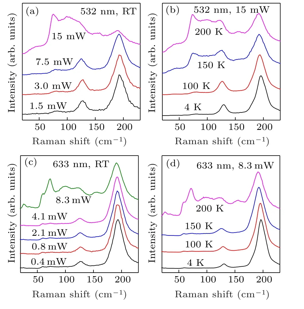
Fig. 3. Laser power- and temperature-dependent conversion of SnSe2 to SnSe. (a)Raman spectra of SnSe2 after a 532 nm laser irradiation with different laser powers at room temperature(RT).(b)Raman spectra of SnSe2 after a 532 nm laser irradiation with power of 15 mW at different substrate temperatures. (c) Raman spectra of SnSe2 after a 633 nm laser irradiation with different laser powers at RT.(d)Raman spectra of SnSe2 after a 633 nm laser irradiation with power of 15 mW at different substrate temperatures.
3.4. Patterned conversion of SnSe2 to SnSe
HRTEM was used to further confirm that after laser irradiation, SnSe2is converted to SnSe. After laser irradiation,burnt holes with a diameter of 1-2 µm are clearly observed in the TEM image of SnSe2flake,as shown in Fig.4(a). The lattice resolved HRTEM image of the the region at the edge of the burn hole after laser irradiation is shown in Fig.4(b). The lattice fringes indicate a perfect atomic structure with a lattice spacing of 3.02 °A,corresponding to the(0¯11)planes of a orthogonal-phase SnSe.[24]As discussed above,only the center region under laser irradiation can be converted. Therefore,the local conversion of SnSe2to SnSe at predefined regions can reach a higher spatial resolution than the laser spot. Figure 4(c)shows the AFM image of SnSe2flake after a 532 nm laser irradiation with power of 2 mW.The depth of burnt holes is~1.5 nm and the diameter is smaller than 200 nm,which is much smaller than the diameter of the laser spot (~500 nm)with the 100× objective lens. To demonstrate the capability of creation of in-plane SnSe2-SnSe p-n junction by this local phase conversion technique,patterned conversion of SnSe2to SnSe was performed by point-by-point laser irradiation on SnSe2flakes. As shown in Fig. 4(d), an “IOP” pattern is clearly observed. Lower inset shows the Raman mapping at 69 cm-1of the pattern, indicating that the irradiation area is completely converted into SnSe.
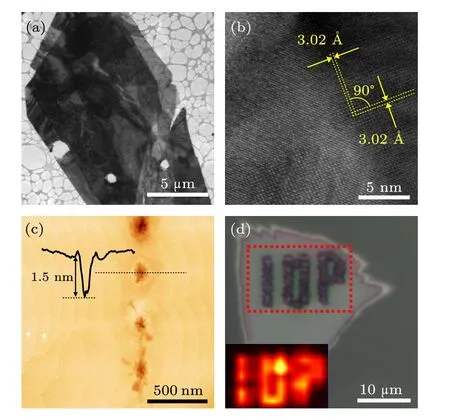
Fig.4. (a)TEM image of the SnSe2 flake after laser irradiation. Laser burnt holes can be clearly observed. (b) The lattice-resolved TEM image of the region at the edge of the burn hole after laser irradiation. (c)AFM image of SnSe2 flake after a 532 nm laser irradiation with power of 2 mW.(d)Optical microscope image of SnSe2 nanoflake after patterned laser-induced phase conversion. The lower inset shows the Raman mapping image of the pattern,indicating that the irradiation area is completely converted into SnSe.
4. Conclusion
In summary, we have developed a novel method to locally convert n-type SnSe2to p-type SnSe. This inversion is confirmed by collecting Raman spectra on SnSe2flakes before and after laser irradiation. The physical mechanism of this phase conversion is revealed by measuring the Raman spectra of SnSe2flakes after laser irradiation performed at different temperatures, indicating that it is the laser heating effect induces the removal of Se atoms from SnSe2to convert SnSe2to SnSe. High-resolution TEM image of SnSe2flakes after laser irradiation shows atomic structure of SnSe, further confirming the conversion of SnSe2to SnSe. The successful patterned conversion of SnSe2to SnSe shows that this laser induced phase conversion technique has a high spatial resolution better than the laser spot and enables the creation of micronsized in-plane p-n junction at predefined region.
Acknowledgments
This work was supported by the National Key Research&Development Project of China(Grant Nos.2016YFA0202300 and 2018FYA0305800), the National Natural Science Foundation of China (Grant No. 61888102), Strategic Priority Research Program of Chinese Academy of Sciences (Grant Nos.XDB30000000 and XDB28000000),and Youth Innovation Promotion Association of Chinese Academy of Sciences(Grant No.Y201902).
- Chinese Physics B的其它文章
- Quantum walk search algorithm for multi-objective searching with iteration auto-controlling on hypercube
- Protecting geometric quantum discord via partially collapsing measurements of two qubits in multiple bosonic reservoirs
- Manipulating vortices in F =2 Bose-Einstein condensates through magnetic field and spin-orbit coupling
- Beating standard quantum limit via two-axis magnetic susceptibility measurement
- Neural-mechanism-driven image block encryption algorithm incorporating a hyperchaotic system and cloud model
- Anti-function solution of uniaxial anisotropic Stoner-Wohlfarth model