
The 50 nm-thick yttrium iron garnet films with perpendicular magnetic anisotropy
2022-04-12 03:48ShuyaoChen陈姝瑶YunfeiXie谢云飞YucongYang杨玉聪DongGao高栋DonghuaLiu刘冬华LinQin秦林WeiYan严巍BiTan谭碧QiuliChen陈秋丽TaoGong龚涛EnLi李恩LeiBi毕磊TaoLiu刘涛andLongjiangDeng邓龙江
Chinese Physics B 2022年4期
Shuyao Chen(陈姝瑶) Yunfei Xie(谢云飞) Yucong Yang(杨玉聪) Dong Gao(高栋) Donghua Liu(刘冬华)Lin Qin(秦林) Wei Yan(严巍) Bi Tan(谭碧) Qiuli Chen(陈秋丽) Tao Gong(龚涛) En Li(李恩)Lei Bi(毕磊) Tao Liu(刘涛) and Longjiang Deng(邓龙江)
1National Engineering Research Center of Electromagnetic Radiation Control Materials,University of Electronic Science and Technology of China,Chengdu 610054,China
2School of Materials and Energy,University of Electronic Science and Technology of China,Chengdu 610054,China 3School of Electronic Science and Engineering,University of Electronic Science and Technology of China,Chengdu 611731,China
Keywords: spintronics,perpendicular magnetic anisotropy,magnetic thin film,deposition by sputtering
1. Introduction
Magnetic films with perpendicular magnetic anisotropy(PMA) enable the stabilization of skyrmions under zero magnetic field,[1,2]the manipulation of magnetization via damping-like spin-orbit torque(SOT),[3,4]and the realization of complex magnonic data processing circuits based on backward volume spin wave.[5]Parallelly,magnetic damping(α)is another key parameter of magnetic thin films.Lowerαwill result in lower critical current density for SOT magnetic moment switching,faster speed for magnetic domain wall or skyrmion motion,and lower decay rate for spin waves propagation.[6,7]Therefore, the realization of magnetic thin films possessing spontaneous out-of-plane magnetization and lowαsimultaneously could open new perspectives for both spintronics and magnonics fields.
Under this context, rare-earth ion garnets have attracted intensive interest in recent years. This is thanks to their insulating nature,which results in much lower damping than magnetic metals due to the absence of electron-magnon interaction. At the same time, their relatively large magnetostriction constant makes it not difficult to obtain PMA in thin films via introducing tetragonal lattice distortion.[7]So far,many research groups have obtained PMA in different magnetic garnet thin films by growing them on lattice mismatched non-magnetic garnet substrates.[8-18]Particularly, there are several works indicating that yttrium iron garnet (YIG) thin films, which have lower inherentαthan any other magnetic material,[19]could obtain perpendicular magnetization if an appropriate non-magnetic garnet substrate was chosen.[20-23]For example,the PMA YIG films grown on GSGG by Dinget al.[23]haveαlower than 5×10⁻⁴. Nevertheless, due to the small magnetostriction coefficient of YIG, a relatively large lattice-mismatched substrate with YIG was always selected in these works. This makes it is difficult to suppress the strain relaxation and obtain PMA in YIG thin films with thicknesses of more than 20 nm, which will be a severe drawback for the applications of PMA YIG films in the future. For example, spintronic and magnonic devices with such a thin YIG film will have very limited process compatibility. Moreover,it would be not easy to read out the state of magnetization or spin wave in such a thin insulating YIG film,as the signal strength is based on spin Hall magnetoresistance,spin Seebeck effect,spin pumping effect,and static or dynamic diploe field which all scale with the thickness of the ferromagnetic layer.
In this work,we have successfully obtained PMA in YIG films epitaxially grown on Gd2.6Ca0.4Ga4.1Mg0.25Zr0.65O12(sGGG) substrates, with a moderate amount of lattice mismatch with YIG.With the optimization of the growth and annealing conditions,the homogenous in-plane tensile stress can be well sustained in the YIG films with the thicknesses up to 50 nm,which represents the thickest pure YIG film with PMA reported thus far. Our work is of great technical importance for the development of high-speed energy-efficient spintronic and magnonic devices.
2. Methods
YIG films with thicknesses ranging from 22 nm to 50 nm were grown on[111]-oriented single-crystal sGGG substrates by radio-frequency sputtering. The deposition was carried out at room temperature, at a rate of about 0.11 °A/s; prior to sputtering, the sputtering chamber had a base pressure of 5.0×10⁻⁸Torr, and the working gas was high pure Ar at a pressure of 7×10⁻³Torr. The deposited YIG film was then annealed at 800°C for 3 h with a pure oxygen pressure of 10 Torr. Notably, in order to obtain enough magnetoelastic anisotropy in the YIG film to overcome the shape anisotropy,and at the same time ensure the homogenous strain to be well preserved, we selected a substrate sGGG that has a moderate amount of lattice mismatch value (~0.9%) with that of YIG.Apart from that,instead ofin-situannealing on the sputtering sample holder, the as-deposited YIG films were postannealed in a separate tube furnace, which has a large space with uniform temperature to avoid temperature gradient along the thickness direction. For the YIG samples presented in this work, the crystalline structure and film thickness were characterized through x-ray diffraction (XRD) and x-ray reflectivity (XRR) measurements, respectively. The static and dynamic magnetic properties were quantitatively studied using a vibrating sample magnetometer(VSM)and a ferromagnetic resonance(FMR)system,respectively. The spin transparency at the surface was also checked by spin pumping induced inverse spin Hall effect(SP-ISHE)measurement using a YIG/Pt bilayer sample.
3. Results and discussion
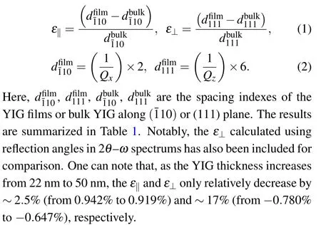
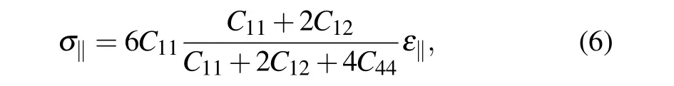
Figure 1(a) shows the XRR spectra obtained from four YIG samples,which will be presented in the following. From XRR results, the thicknesses (t) of the four YIG samples are determined to be 22±1 nm, 31±1 nm, 45±1 nm, and 50±1 nm. For accuracy, we have also double-checked the thicknesses of these YIG films by cross-sectional scanning electron microscope (SEM) measurements; and the result of the 50 nm YIG is shown in the inset of Fig.1(a). Figure 1(b)presents the standard 2θ-ωXRD scans near the sGGG(444)peak. One can note that only a diffraction peak corresponding to YIG (444) peak is evident. Except for the thickest 50 nm YIG, Laue fringes are present in all the other three samples,indicating the high crystalline quality of the YIG films with a sharp interface and smooth surface. In addition, the YIG(444)peaks are located at the right side of the diffraction angle of bulk YIG material (vertical black dashed line), indicating the decrease of the lattice constant nominal to the film plane and formation of out-of-plane(OOP)compressive strain in the YIG films,which support the goal of achieving PMA.This is in line with the expectation of growing YIG thin films following the in-plane (IP) lattice of the substrate with a larger lattice constant. More interestingly, in contrast to the widely observed XRD peak position shift due to the increase of the YIG film thickness in previous reports,[23,24]the (444) peak position of the YIG samples concerned in this paper almost does not change, even when the YIG is as thick as 50 nm.This can be more clearly seen from the Bragg law calculated OOP lattice constant as a function of the YIG thickness, as shown in Fig. 1(c). The aforementioned XRD results might serve as a good evidence indicating that the epitaxial growthinduced strain in our YIG films can be well preserved even when the YIG is as thick as 50 nm. Therefore, it is possible for us to obtain highly stressed homogenous PMA YIG films with thickness even up to 50 nm.
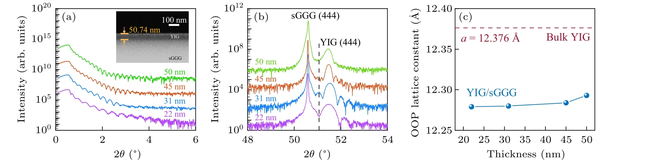
Fig.1. XRD results of YIG films grown on sGGG substrates. The inset: SEM micrographs of the YIG (50.74 nm). (a) XRR spectra; (b)2θ-ω spectra.The vertical dashed line represents the diffraction angle of bulk YIG(444).(c)OOP lattice constant as a function of the YIG film thickness.The horizontal dashed line illustrates the lattice constant of bulk YIG.The inset in(a)is the cross-sectional SEM image of the 50 nm YIG.
In order to more comprehensively study the strain distribution in the YIG films,especially for the details of the strain in the film plane,high-resolution reciprocal space map(RSM)measurements around the peak(468)were also carried out,the results of which are shown in Fig.2. For comparison,the peak(468) of bulk YIG is also marked out with a red cross in the figures. There are several important results that can be distinguished from these RSM graphs. Firstly,as will be presented shortly,the OOP strain obtained from theQz(486)‖[111]values can well reproduce that of YIG (111) reflection angle in 2θ-ωspectra. This indicates the reliability of our RSM results. Secondly,Qx(486)‖[¯110], which reflects the IP lattice constant, is almost the same as that of the sGGG for all the YIG films. This indicates the pseudo-morphic-growth nature of our YIG films on sGGG substrates, which is the source of the IP tensile and OOP compressive strain in the YIG films.Thirdly,the peak(468)of these four YIG samples have a very similar shape and locate at almost the same position that is far apart from that of the bulk YIG.This further indicates that the strain in our highly stressed YIG films grown on sGGG substrate only relaxes very little even when the YIG is 50 nm thick.
To more quantitatively study how the strains in YIG films change with their thickness,we calculate both the IP strain(ε‖)and OOP strain(ε⊥)using the following equations:
In the next, the room temperature static and dynamic magnetic properties of the YIG films were studied by VSM and FMR measurements. Figure 3 shows the IP and OOP hysteresis loops of the four YIG thin films with different thicknesses. As presented, all the four YIG are much harder to be saturated as the applied magnetic field is IP than in the case of OOP.Particularly, for the 22 nm YIG films, the OOP hysteresis loop is square with a remnant-to-saturation magnetization ratio (Mr/Ms) of~95%, whereas the IP hysteresis loop is slanted with a saturation field of more than 400 Oe,indicative of a standard magnetic film with strong PMA.As for the thicker YIG films,theMr/Msin their OOP hysteresis loops become much smaller.Nevertheless,their IP saturation fields are still higher than 400 Oe,much higher than the OOP saturation fields,which is still true for the 50 nm YIG.The above results indicate that the easy magnetization axes of the four YIG films are all lying OOP. Regarding the unsquared OOP loops observed in the relatively thick YIG films,it most probably is the result of the formation of complex magnetic or domain structures at remnant state,which is well worthy of further studies.For example,the OOP loop of the 50 nm YIG resembles that of metallic magnetic films with skyrmions crystal or isolated skyrmions.[25-27]Besides,it also needs to be noted that the saturation magnetization(Ms)of the YIG films is slightly lower than that of bulk YIG,which might be due to the stoichiometry variance,iron and oxygen defects,or strain.

Table 1. Summary of the stains in the YIG films,which are determined from XRD 2θ-ω spectra(ε⊥(2θ))or RSMs(ε⊥(Qz)and ε‖(Qx)).

Fig.2. High-resolution reciprocal space maps of symmetric scan around the peak(486). The red cross represents the peak(468)of bulk YIG.

Fig.3. Hysteresis loops of the YIG films measured with magnetic field applied in-plane and out-of-plane.
To determine the value of PMA field(Hk),the FMR field(HFMR)as a function of the magnetic field direction was measured with a 9.6 GHz microwave cavity, the results of which are shown in Fig.4(a). The dots are experiment data,whereas the lines are fits to[28,29]

Here,K1andλ111are the first-order cubic anisotropy constant(-6.1×10³erg/cm3)[31]and the magnetostriction coefficient(-2.4×10⁻⁶),[32]respectively.σ‖is the IP stress,which can be obtained by[33]

Three results can be evident from Fig. 4(a) and Table 2.Firstly,it is unambiguous that all the four YIG films are spontaneously magnetized OOP, which could be clarified either by the smaller OOPHFMRthan that of IP or by the negative sign of 4πMeff. Secondly,Hkagrees reasonably well with the value ofHck, indicating that the dominant source of PMA is strain. The slight deviation could have been caused by the extra PMA contributions like crystal magnetic anisotropy or growth-induced anisotropy. This is different from the case of BixY3-xIG films in Ref.[36],where the PMA is dominant by growth-induced anisotropy. The reason caused the difference in the two materials is not clear,which requires further investigations. Thirdly,as the YIG thickness increases from 22 nm to 50 nm, theHkdecreases only by~10%. It is in accordance with the RSM results presented above and again indicates the robustness of the strain and the strain-induced PMA in our YIG films.
In consideration of the importance of damping value(α)and surface spin transparency(or interfacial spin mixing conductance) in YIG films for applications, we also measuredtheαof the 22 nm and 50 nm YIG, as well as the damping enhancement and SP-ISHE with the deposition of a 3 nm Pt on the 22 nm YIG. Figure 4(b) presents the peak-to-peak FMR linewidth(ΔH)of the YIG(22 nm)and YIG(22 nm)/Pt(3 nm), which are obtained from the Lorenz fittings of the FMR curves measured using a coplanar waveguide(CPW).[35]The dots are experimental data, whereas the lines are the fits to[29]
Table 2. Magnetic properties of YIG thin films grown on sGGG substrates.

Fig.4. The HFMR and SP-ISHE results. (a)HFMR as a function of the magnetic field angle θ. (b) ΔH as a function of frequency f, for a bare YIG(22 nm) and YIG (22 nm)/Pt (3 nm). The inset: VSP-ISHE as a function of magnetic field for YIG(22 nm)/Pt(3 nm).
where ΔH0is the inhomogeneous linewidth broadening. From the fit, theαof the 22 nm bare YIG is determined to be 4.48×10⁻³. This value is an order of magnitude larger than the reported value of PMA YIG with thickness~10 nm by Dinget al.[23]and PMA Bi:YIG with thickness~20 nm by Soumah1et al.,[36]nevertheless it is still much smaller than any other PMA magnetic thin film materials.[13-15]It is also worthy to note that theαof the 50 nm YIG is 3.69×10⁻³,even slightly smaller than that of the 22 nm YIG. The gentle strain relief in 50 nm YIG seems to not affect its dynamic magnetic properties. Then, after deposition of 3 nm Pt on the 22 nm YIG, the damping has been enhanced to beαYIG/Pt=6.3×10-3,due to the spin pumping effect.[37]The interfacial spin mixing conductanceg↑↓in YIG (22 nm)/Pt(3 nm)can be determined to be 3.28×10¹⁸m-2using[38]
wheregandµBrepresent Lande’sg-factor and Bohr magneton,respectively.This value is compatible with that of the previously reported interface between Pt and IP magnetized YIG grown on GGG substrate.[39-41]This indicates good spin transparency at the surface of our PMA YIG films,which could be further proved by the strong SP-ISHE voltage signal(VSP-ISHE)obtained using the same YIG (22 nm)/Pt (3 nm) sample. As shown in the inset of Fig. 4(b), theVSP-ISHEobtained with a microwave power of 20 dBm is~16 µV, which is compatible as well with that of the previously reported value achieved using YIG/Pt grown on GGG substrate.[42]
4. Conclusion and outlook
In summary,our work has proved the feasibility of using sGGG substrate to grow thick YIG films simultaneously possessing PMA and low damping that are desired for the applications of high-speed energy-efficient spintronic and magnonic devices. Therefore,our work is of technical importance. The key taken away of this achieved advancement could be that the sGGG has a moderate lattice mismatch with YIG, which can make YIG film obtain enough magnetoelastic anisotropy to overcome shape anisotropy and at the same time do not have the problem of excessive strain-induced stress relief as the increase of film thickness. In terms of potential device applications of PMA YIG films, the following future works are of great,immediate interest.(1)There is still a large space for the improvement ofαin our PMA YIG films. Further optimizing the growth conditions to reduceαis worth studying. (2)The direct evidence for the hosting of skyrmions in low damping magnetic insulators is still under investigation. As discussed above,the OOP hysteresis loop of the 50 nm PMA YIG looks very similar to that of previously reported magnetic skyrmions materials. It would be interesting to image the magnetic domain structure of our PMA YIG films. (3)Study of the spinorbit-torque driven moment switch or domain wall motion in PMA YIG films, especially by the spin current from materials with strong charge-to-spin conversion efficiency,would be interesting for memory device applications. (4) The generation of backward volume spin waves and realizing their longdistance controllable propagation in PMA YIG films will provide important implications for potential applications of spin wave logic devices.
Acknowledgements
This work was supported by the National Natural Science Foundation of China (Grant Nos. 52072060 and 52021001), the National Key R&D Program of China (Grant No. 2021YFB2801600), and the China Postdoctoral Science Foundation(Grant No.2021M700679).
- Chinese Physics B的其它文章
- Quantum walk search algorithm for multi-objective searching with iteration auto-controlling on hypercube
- Protecting geometric quantum discord via partially collapsing measurements of two qubits in multiple bosonic reservoirs
- Manipulating vortices in F =2 Bose-Einstein condensates through magnetic field and spin-orbit coupling
- Beating standard quantum limit via two-axis magnetic susceptibility measurement
- Neural-mechanism-driven image block encryption algorithm incorporating a hyperchaotic system and cloud model
- Anti-function solution of uniaxial anisotropic Stoner-Wohlfarth model