
Edge assisted epitaxy of CsPbBr3 nanoplates on Bi2O2Se nanosheets for enhanced photoresponse
2022-04-12 03:45HaotianJiang蒋浩天XingXu徐兴ChaoFan樊超BeibeiDai代贝贝ZhuodongQi亓卓栋ShaJiang蒋莎MengqiuCai蔡孟秋andQinglinZhang张清林
Chinese Physics B 2022年4期
Haotian Jiang(蒋浩天), Xing Xu(徐兴), Chao Fan(樊超), Beibei Dai(代贝贝),Zhuodong Qi(亓卓栋), Sha Jiang(蒋莎), Mengqiu Cai(蔡孟秋), and Qinglin Zhang(张清林)
Key Laboratory for Micro-/Nano-Optoelectronic Devices of Ministry of Education,School of Physics and Electronics,Hunan University,Changsha 410082,China
Keywords: Bi2O2Se,heterostructures,photogenerated carriers,photoresponse
1. Introduction
Two-dimensional (2D) semiconductor materials have attracted extensive research interest for both the fundamental physics researches and the practical applications in electronic and optoelectronic devices, due to their unique optical and electrical properties.[1-8]Recently,Bi2O2Se,an emerging 2D material,has been proved to possess typical narrow bandgap,high carrier mobility and superior air stability, which makes it a promising candidate for high-performance devices, such as field effect transistors (FETs), broadband photodetectors(PDs)and ultrafast photodetection.[9-20]Because the heterointerfaces directly determine the operation of modern electronic devices,[21-24]the fabrication of Bi2O2Se-based heterostructures is crucially important for practical applications of the related devices.
Up to date, the combination of Bi2O2Se with other 2D materials including graphene,MoSe2and WSe2has been applied to realize the multifunctional electronics, e.g., the bidirectional all-optical synapses or broadband PDs with high light on/off ratio and fast response.[25-28]Although the high-quality interface may be achieved with two disparate layered materials (2D-2D heterostructures) due to their atomically smooth surfaces without dangling bonds, the limited quantity greatly restricts them to meet the requirements of various functional applications. Moreover, these reported Bi2O2Se-based 2D-2D heterostructures were fabricated with the manual micromanipulation techniques assisted by the optical microscope,which still suffers from the poor positional controllability and low efficiency.[29,30]Consequently, the highly efficient integration of 2D materials with non-layered ones is indispensable to the extended applications beyond 2D-2D heterostructures. Luoet al.reported that the sensitization of Bi2O2Se nanoplates with PbSe quantum dots (QDs) could expand the photoresponse spectral range of Bi2O2Se-based PDs to the wavelength of 2 µm with the response time 300 times faster than PbSe QDs.[31]Although a remarkable enhancement to the responsivity may be obtained with the sensitization due to the photogating effect, the grain boundaries among the stacked QDs as well as the weakly interfacial coupling between QDs and the layered materials may inevitably decrease the carrier transfer efficiency from the sensitizer to the channel material.[32-34]The epitaxial growth of non-layered semiconductors on 2D materials exhibits great potential in efficiently constructing the 2D-based heterostructures high-quality heterointerface,where the dangling-bond-free surfaces of the layered structures are favorable to the growth of epitaxial materials on it without strict lattice match.[3,35-37]Although the various non-layered materials have been epitaxially grown on the traditional 2D materials,[33,38,39]it is still challenging to direct epitaxy of them on Bi2O2Se nanosheets.
CsPbBr3,one of the all inorganic metal halide perovskite,has been proved to possess strong visible light absorption,bipolar transport, long carrier diffusion distance, etc., which is ideal for the light light-absorbing layer.[22,40-42]Furthermore, the integration of CsPbBr3with 2D materials, such as MoS2,WSe2or WS2,may result in the ultrafast charge transfer from CsPbBr3to the layered materials, which is favorable for the high performance optoelectronic devices based on 2D materials.[43,44]Nohet al.fabricated the devices with MoS2-CsPbBr3quantum dots hybrid which exhibited~4 times and~17 times increase, respectively, in the field effect mobility and photoresponsivity under light irradiation than those prepared without the perovskite QDs and without light irradiation.[45]Zhanget al.reported a photodetector based on CsPbBr3nanocrystal/monolayer MoS2, with a high photoresponsivity of 6.40×10⁵mA·W-1, an external quantum efficiency of 1.50×10⁵%,and a specific detectivity of 3.38×10¹¹Jones at zero gate voltage.[46]Although great progress has been made on the theory and application of the hybrids of CsPbBr3-layered transition metal dichalcogenides,the study of the heterostructures of CsPbBr3-Bi2O2Se is still in the initial stage.
Here, we report the high-quality CsPbBr3nanoplate-Bi2O2Se nanosheet heterostructure synthesized via a twostep chemical vapor deposition (CVD) route. CsPbBr3nanoplates were selectively grown at the edge of the Bi2O2Se sheet, when the pre-synthesized Bi2O2Se nanoplates were annealed in the evaporated CsBr and PbBr2atmosphere.The epitaxial relationship between CsPbBr3plates and the Bi2O2Se sheets were verified to be [200]Bi2O2Se||[110]CsPbBr3and [110]Bi2O2Se||[200]CsPbBr3by a transmission electron microscopy (TEM). The control experiments demonstrate the dangling bonds at the edge of Bi2O2Se sheets play a critical role in the nucleation of CsPbBr3. The microphotoluminescence (µ-PL) characterizations reveal that the contact of CsPbBr3with Bi2O2Se results in a significant PL quenching. The ultraviolet photoelectron spectroscopy(UPS)and Kelvin probe measurements reveal the type-I band alignment at the hetero-interface,which makes the photogenerated carrier transfer from CsPbBr3to Bi2O2Se and hence the PL quenching. Importantly, the photodetectors based on the heterostructures have the responsivity of 7.7 A/W,which is more than 4 times higher than that of the devices based on the pristine Bi2O2Se (1.8 A/W). This can be contributed to the high absorption coefficient of CsPbBr3and the efficient carrier transfer from CsPbBr3to Bi2O2Se. Additionally, the devices based on the heterostructures exhibit fast response time of 4.4 ms and 2.8 ms for the rise and decay time,respectively.The direct epitaxy of CsPbBr3plate on Bi2O2Se sheet paves the way to fabricating the Bi2O2Se based heterostructures with high efficiency, which promotes the practical application of Bi2O2Se in optoelectronic devices.
2. Experimental details
Sample preparation CsPbBr3nanoplate-Bi2O2Se heterostructures were synthesized by a two-step CVD route.Firstly, Bi2O2Se nanosheets were synthesized on a freshly cleaved mica substrate by a furnace with 1-inch diameter quartz tube. The Bi2O3powder was put in the center of the heat zone, Bi2Se3powder was put upstream 10 cm away from the center, and the mica was placed downstream 12 cm away from the center. Before the growth, 200 sccm N2gas flow was used to flush the system for 30 min to exhaust air.Then, the furnace was heated to 620°C and kept constant for 30 min to synthesize Bi2O2Se nanosheets. In the whole process, the pressure in the furnace was controlled at about 2500 Pa. Secondly, CsPbBr3nanoplate-Bi2O2Se nanosheet heterostructures were synthesized by annealing the pre-grown Bi2O2Se nanosheet in the evaporated PbBr2and CsBr atmosphere. The mixed PbBr2and CsBr powders(molar ratio 1:1)was placed at the center of the heating zone,and the pre-grown Bi2O2Se nanosheets were placed at the downstream. Then the furnace was heated to 550°C and kept for 10 min to grow CsPbBr3nanoplate on Bi2O2Se nanosheet.
Characterizations The morphologies and crystal structure of CsPbBr3nanoplate-Bi2O2Se heterostructures were characterized by an optical microscope, SEM (Hitachi, S-4800), XRD (Shimadzu, XRD-6100), and TEM (FEI, Tecnai G2 F20). The Raman and PL measurements were performed with a confocal microscope (Witec Alpha 300) under the excitation of a focused 473 nm laser.
Device fabrication The device of CsPbBr3nanoplate-Bi2O2Se was preparedin situon the grown mica substrate.Two small pieces of Sn/Bi alloy(melting point:about 148°C)foils were manipulated with a micro probe under the optical microscope to contact with the Bi2O2Se sheet to act as the source and drain. Then, the devices were annealed at 150°C for 20 s to improve the electrical contact. Finally, the electronic characteristics of the obtained devices were measured by a probe table with a semiconductor parameter analyzer(Agilent, B4155C) and the photoresponse time was recorded by an oscilloscope(TDS5054B).
3. Results and discussion
Figure 1(a)shows the optical microscope image of a representative Bi2O2Se nanosheet grown on the mica substrate.The quadrate sheet with the side length of~25 microns agrees well with the tetragonal phase of Bi2O2Se.[20,48]After the presynthesized Bi2O2Se sheets were annealed in the evaporated CsBr and PbBr2atmosphere,CsPbBr3square nanoplates with the side length of several microns were only grown at the edges of Bi2O2Se sheets(see Figs.1(b)and S1 in the supporting information), while the inner area of the Bi2O2Se sheets keeps the clean surface as the pristine ones,which indicates that the edges of Bi2O2Se sheets play an important role in the nucleation of CsPbBr3. Interestingly, a diagonal of each of the CsPbBr3plates is parallel with the side of Bi2O2Se sheet. In consideration of the cubic phase of CsPbBr3and tetragonal phase of Bi2O2Se, it can be deduced that the [110]CsPbBr3is parallel with[100]Bi2O2Se,which will be further discussed latter. The thickness of the Bi2O2Se sheet and epitaxial CsPbBr3plate were measured by an atomic force microscopy(AFM)to be about 25 and 85 nm, respectively (see Fig. S2 in the supporting information). Figure 1(c) gives the locally amplified scanning electron microscope(SEM)image of the heterostructure. The corresponding elemental mappings (see Fig. 1(d))clearly show that Bi and Se elements distribute uniformly across the entire upper part, while Pb and Br only distribute in the square area with its diagonal parallel with the side of Bi2O2Se plate,which results in one half of the CsPbBr3plate being on the Bi2O2Se (upper part) and the other half being on the mica (lower part). To check the crystal phases, the xray diffraction(XRD)patterns of the obtained heterostructures were measured (shown in Fig. 1(c)). The diffraction peaks can be respectively indexed to cubic CsPbBr3(PDF#75-0412)and tetragonal Bi2O2Se (PDF# 73-1316), where the sharp diffraction peaks demonstrate the high crystal quality of the as-grown sample. Additionally,only the peaks of{200}sPbBr3and{002}Bi2O2Secan be observed,indicating that the CsPbBr3plates were grown with the(200)CsPbBr3plane interfacing with the surface of(002)Bi2O2Se.

Fig. 1. (a) Optical microscope image of a representative Bi2O2Se nanoplate grown on a mica. (b) Optical microscopy images of CsPbBr3 nanoplate-Bi2O2Se nanosheet heterostructures grown on a mica. (c)Locally amplified SEM image of the heterostructure. (d)EDS mapping of Bi,Se,Pb and Br elements measured from the area of(b). (e)XRD spectra of the heterostructures.
To reveal the detailed epitaxial relationships between the CsPbBr3plates and the Bi2O2Se sheets, TEM were used to check their microstructures. Figure 2(a) shows the lowmagnification TEM image of the CsPbBr3-Bi2O2Se heterostructure transferred onto a Cu grid. It can be seen that CsPbBr3plate contacts with the edges of Bi2O2Se sheet with an angle of 45°between the sides of these two phases,which is consistent with the results in above optical microscope and SEM images. Figures 2(b) and 2(c) are the high-resolution TEM (HRTEM) images corresponding to the Bi2O2Se and CsPbBr3region marked by the solid- and dotted-line rectangle in Fig.2(a),respectively. The lattice spacing can be measured to be 0.195 and 0.421 nm for (200)Bi2O2Se(Fig. 2(b))and (110)CsPbBr3, respectively (Fig. 2(c)). The corresponding selected-area electron diffraction (SAED) patterns (insets in Figs. 2(b) and 2(c)) further confirm the tetragonal and cubic crystal for the Bi2O2Se and CsPbBr3, respectively.Figure 2(d) gives the SAED pattern measured at the position marked by the circle in Fig. 2(a) with the electrons incident along the [001]Bi2O2Seand [001]CsPbBr3direction.Two sets of spots can be clearly distinguished for tetragonal Bi2O2Se (red square) and cubic CsPbBr3(green square),respectively. The epitaxial relationships between Bi2O2Se and CsPbBr3can be deduced to be [200]Bi2O2Se||[110]CsPbBr3and [110]Bi2O2Se||[200]CsPbBr3in two in-plane directions.This directional relationships are consistent with the nearly same lattice mismatch factors (defined asf= [(dBi2O2SedCsPbBr3)/dBi202Se× 100%)] of [200]Bi2O2Se||[220]CsPbBr3(-6.75%) and [110]Bi2O2Se||[200]CsPbBr3(-6.75%), wheredBi2O2Se(200)=0.195 nm,dBi2O2Se(110)=0.275 nm(PDF#73-1316),dCsPbBr3(220)=0.207 nm anddCsPbBr3(200)=0.294 nm(PDF# 75-0412). These result in the same energy barriers for aligning the adatoms of CsPbBr3along [200]Bi2O2Seand [110]Bi2O2Se, which contribute to the formation of square CsPbBr3plate on the Bi2O2Se sheet(see the atomic arrangement schematic of the heterostructure in Fig.2(e)).
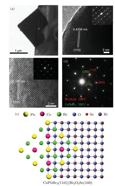
Fig.2. (a)Low-magnification TEM image of CsPbBr3 nanoplate-Bi2O2Se heterostructure transferred onto a Cu grids. (b) HRTEM image of the area marked with solid line rectangle in (a). Inset: The corresponding SAED pattern. (c) HRTEM image of the area marked with dotted line rectangle in (a). Inset: The corresponding SAED pattern. (d) SAED pattern measured at the position marked with a circle in (a). (e) Atomic arrangement schematic of the CsPbBr3 nanoplate-Bi2O2Se nanosheet viewed from[001]Bi2O2Se||[001]CsPbBr3.
To further confirm the initial nucleation location of the CsPbBr3plates, the Bi2O2Se film with millimeter size was used as the epitaxial substrate. As shown in Fig.S3(a), there are many cracks in the film, which may be resulted from the large strain generated during the growth process. Interestingly,after the film was annealed in the evaporated CsBr and PbBr2atmosphere, many CsPbBr3plates appear and all of them are selectively grown along the cracks with the same orientations(see Fig.S3(b)). Because both sides of the crack are Bi2O2Se,this result clearly reveals that the CsPbBr3plates primarily nucleate at the edge of Bi2O2Se sheet. We contribute this to the unsaturated atoms at the edges of Bi2O2Se sheets(see the crystal structure schematic in Figs. S4) which provide the nucleation sites for CsPbBr3, and then promote the growth of the plates on Bi2O2Se surface according to the defined epitaxial relationships. Figure S5 gives the SEM images of the CsPbBr3plates grown on thin and thick Bi2O2Se sheets, measured with the tilted view. For the thin Bi2O2Se sheet (Fig. S5(b)), the square CsPbBr3plates stretch across the edge of the Bi2O2Se sheet and contact with both mica and Bi2O2Se. However, for the thick Bi2O2Se sheet with the thickness of about 2 µm (Fig. S5(a)), right triangle CsPbBr3plates were only grown on the mica with the right-angle side contacting with the side wall of Bi2O2Se sheet, where steps were formed due to the larger thickness of Bi2O2Se sheet than that of CsPbBr3plates. These further reveal that the initial nucleation of CsPbBr3was assisted by the edges of Bi2O2Se sheets, where the adatoms of CsPbBr3connect with the dangling bonds at the edge of Bi2O2Se sheets with(200)Bi2O2Se||(110)CsPbBr3. The formation of square or righttriangle shape CsPbBr3plates is thermodynamically favorable,because the exposure of{001}CsPbBr3results in the lowest surface energy for a cubic crystal.[22]
It should be noted that all the CsPbBr3plates were aligned along the edge of Bi2O2Se sheet(see Figs.1 and S1),which is quite different from the epitaxy of CsPbBr3nanowires on the surface of Bi2O2Se sheets with the epitaxial relationship of[200]Bi2O2Se||[001]CsPbBr3.[49]We contribute these to the various growth modes controlled by the growth conditions. The wires nucleated in the inner part of Bi2O2Se sheets where the surface of (001) plane is free of dangling bonds, while the plates were grown at the edge of Bi2O2Se sheets with many dangling bonds. Generally, the growth of epilayer on a substrate with chemical bonds requires to overcome much higher energy barrier than that with van der Waals (vdW) force.[50]Consequently, the wires were grown by a vertically physical vapor deposition method with low evaporation (330°C) and growth (220°C) temperature, which resulted in the low precursor supersaturation and low adatom diffusion rate. Differently,the plates were grown by a horizontally chemical vapor deposition routes with high evaporation (550°C) and growth(320°C)temperature,which may lead to high precursor super staturation and high adatom diffusion rate. The high supersaturation can overcome the high energy barrier for the growth of the epilayer on the substrate with dangling bonds, and the higher temperature promotes the diffusion of the adatoms,suppressing the nucleation on the vdW surface.Therefore,the low(high)supersaturation of precursor and low(high)growth temperature contribute to the growth of nanowires(nanoplates)at the inner(edge)of the Bi2O2Se sheets.
Figure 3(a) is the optical microscope image of another CsPbBr3-Bi2O2Se heterostructure.The microphotoluminescence (µ-PL) spectra measured from the different positions on a CsPbBr3plate marked by the spots in Fig. 3(a) are shown in Fig. 3(b). Both µ-PL spectra exhibit a center wavelength of about 522 nm, agreeing well with the band edge emission of CsPbBr3.[51]Differently, the position on the Bi2O2Se sheet(red dot)possesses the eight folder lower emission intensity relative to that on the mica,which indicates the significant PL quenching of CsPbBr3when contacts with Bi2O2Se.Figure 3(c)gives the PL mapping measured from the rectangle area marked in Fig.3(a), with integrating the emission intensity near 522 nm. The whole region of the CsPbBr3plate on Bi2O2Se sheet shows much lower emission intensity than that on the mica (the dashed line denotes the edge of the Bi2O2Se sheet), which further confirms that the contact of CsPbBr3with Bi2O2Se can result in the PL quenching of CsPbBr3.
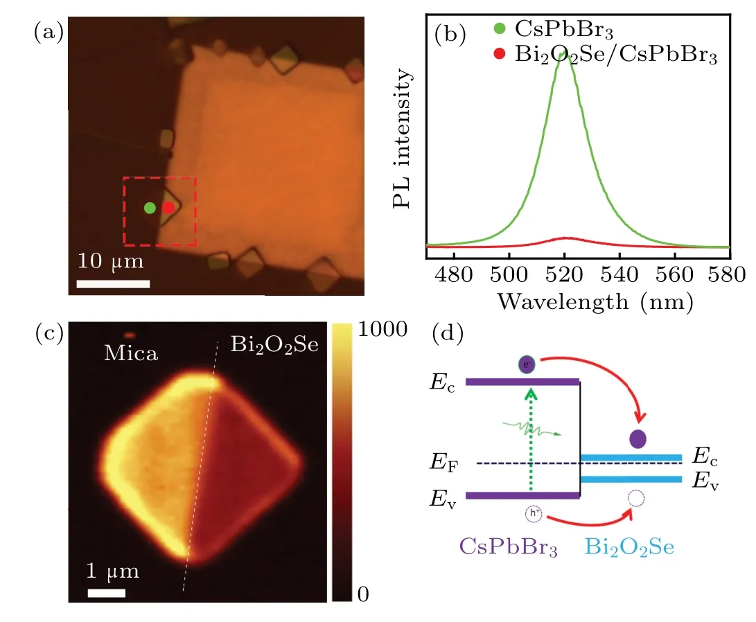
Fig. 3. (a) Optical microscope image of CsPbBr3 nanoplate-Bi2O2Se nanosheet heterostructure. (b) PL spectra measured respectively from the positions marked with red and green dots in(a). (c)PL mapping of marked area with dotted line rectangle in(a). (d)The schematic of the band alignment diagram between CsPbBr3 and Bi2O2Se.
Generally, the PL quenching in the semiconductor heterostructures is resulted from the charge transfer at the hetero-interface, which depends on their interfacial band alignment.[22]In order to obtain the information of band arrangement between CsPbBr3and Bi2O2Se in the heterostructure,UPS measurements were carried out. Combining the valence band spectra and second electron cutoff energy (Ecut)(see Fig. S6 for details), the work functions (W) of CsPbBr3and Bi2O2Se were estimated to be 5.31 eV and 4.69 eV,respectively, according to the formula ofW=hν-Ecut(hν=21.22 eV,Ecutof CsPbBr3and Bi2O2Se are 15.91 eV and 16.53 eV, respectively), and the valence band maximum (VBM) of CsPbBr3and Bi2O2Se are 0.51 eV and 0.64 eV lower than their Fermi levels (EF), respectively.Therefore, type-I band alignment should be formed at the hetero-interface based on the reported bandgaps of CsPbBr3(2.4 eV) and Bi2O2Se (0.8 eV),[22,48]which facilitates both the photo-generated electrons and holes in CsPbBr3injecting into Bi2O2Se and hence the PL quenching of CsPbBr3(see Fig. 3(d)). The UPS results can be further confirmed by the Kelvin probe measurements which show thatWof CsPbBr3and Bi2O2Se are respectively 5.25 eV and 4.83 eV(see Fig.S7),agreeing with the values measured by UPS.Additionally,the excitation of 405 nm laser leaded to a decrease and increase in the potential of Bi2O2Se and CsPbBr3, indicating the n-and p-type conduction of Bi2O2Se and CsPbBr3,respectively.[22,47]These agree well with the relative energy difference between theEFand the VBM measured by the UPS for Bi2O2Se and CsPbBr3. Importantly, the efficient transfer of photo-generated carriers from CsPbBr3to Bi2O2Se promotes the carrier accumulation in Bi2O2Se,which is expected to improve the optoelectronic performance of the devices.[22]
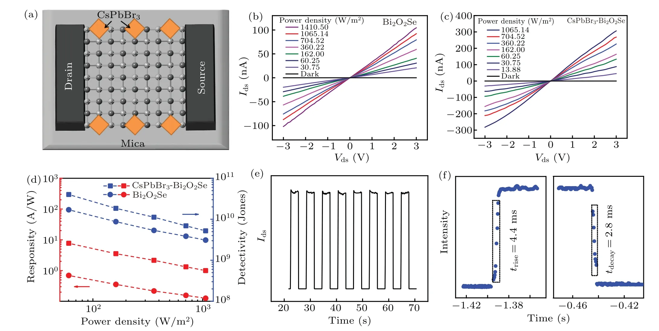
Fig.4.(a)Schematic illustration of CsPbBr3 nanoplate-Bi2O2Se heterostructure based device.(b)and(c)Ids-Vds curves of the photodetectors based on pristine Bi2O2Se and the heterostructure under dark and 450 nm illumination at different incident power densities. (d)The illumination power dependent responsivity and detectivity of the photodetectors based on the pristine Bi2O2Se and the heterostructure. (e)Time-dependent current response of the photodetector based on the heterostructure under repeated on/off light illumination. (f)Time-resolved light response photodetectors based on the heterostructures.
4. Conclusions
In summary, we have successfully synthesized CsPbBr3nanoplates-Bi2O2Se heterostructure by a two-step CVD growth method.The dangling bonds at the edge of Bi2O2Se sheet provide the initial nucleation site of CsPbBr3,and the lattice match control their epitaxial relationships of[200]Bi2O2Se||[110]CsPbBr3and [110]Bi2O2Se||[200]CsPbBr3.The contact of CsPbBr3to Bi2O2Se results in the efficient photogenerated charge transfer from the former to the latter,which agrees with type-I band alignment at the heterointerface. Furthermore,the photodetectors based on the heterostructure possess the responsivity of 7.7 A/W at 60.25 W/m2that is 4 times higher than the ones based on pristine Bi2O2Se plates. This work provides an effective route to grown Bi2O2Se-based heterostructures which have the potential in the application in high-performance optoelectronic devices.
Acknowledgements
The authors are grateful to the National Natural Science Foundation of China (Grant No. 51772088) and Hunan Provincial Innovation Foundation for Postgraduate,China(Grant No. CX20200422), and thank Prof. Huigao Duan for the help of the PL measurements.
- Chinese Physics B的其它文章
- Quantum walk search algorithm for multi-objective searching with iteration auto-controlling on hypercube
- Protecting geometric quantum discord via partially collapsing measurements of two qubits in multiple bosonic reservoirs
- Manipulating vortices in F =2 Bose-Einstein condensates through magnetic field and spin-orbit coupling
- Beating standard quantum limit via two-axis magnetic susceptibility measurement
- Neural-mechanism-driven image block encryption algorithm incorporating a hyperchaotic system and cloud model
- Anti-function solution of uniaxial anisotropic Stoner-Wohlfarth model