
Fast-speed self-powered PEDOT:PSS/α-Ga2O3 nanorod array/FTO photodetector with solar-blind UV/visible dual-band photodetection
2022-04-12 03:48MingMingFan范明明KangLiXu许康丽LingCao曹铃andXiuYanLi李秀燕
Chinese Physics B 2022年4期
Ming-Ming Fan(范明明), Kang-Li Xu(许康丽), Ling Cao(曹铃), and Xiu-Yan Li(李秀燕)
College of Physics and Optoelectronics,Taiyuan University of Technology,Taiyuan 030024,China
Keywords: fast speed,self powered,solar-blind UV/visible photodetection,PEDOT:PSS/α-Ga2O3/FTO
1. Introduction
Nowadays, Ga2O3has been recognized as one kind of star materials for potential solar-blind UV photodetection due to its inherent absorption range in solar-blind UV, such as nonline-of-sight communication, ozone monitoring, light intensity measurement, sterilization, high-temperature flame supervisory control, and missile alarm.[1-3]More recently,multiband photodetection with wider and more photodetection bands shows potential applications in imaging, machine vision,meteorology,surveillance,astronomy,communication,rescue,etc.[4-7]Therefore,to extend the photodetection range of Ga2O3-based photodetectors beyond its inherent absorption range becomes also a research hotspot by alloying or constructing heterojunctions.[8-14]Although Al2O3has been successfully alloyed with Ga2O3to extend its absorption range into shorter wavelength region, constructing proper heterojunctions between Ga2O3and other materials remains a feasible way to realize the extension of its photodetection range into long-wavelength region.[10-14]According to the reported literature, Ga2O3dual-band photodetectors have mainly been investigated in UV region, which shows the other UV band besides the inherent solar-blind UV band.[10-13]However,the further extension of its photodetection range into visible region was seldom investigated.
To realize solar-blind UV/visible dual-band photodetection,Ga2O3should be combined with other visible absorbers to construct heterojunctions. Compared with other inorganic semiconductors, organic semiconductors show advantages in large-scale fabrication, flexibility, cheap and easy integration by spin coating process.[15-18]For example,Ce6(a derivative of natural chlorophyll)was coated onβ-Ga2O3/MoS2to realizeβ-Ga2O3/MoS2/Ce6 DUV/visible dual-band photodetectors with excellent photoresponse properties.[19]Nevertheless,the fabrication processes were complex,including the growth ofβ-Ga2O3film on Si by PECVD, the growth of MoS2by CVD and the further transfer of MoS2on theβ-Ga2O3film.Besides,the dual-band photodetectors should be operated under bias voltages with a slow response time of>2 s. Therefore,more simple fabrication processes should be explored to realize solar-blind UV/visible dual-band photodetectors in a power-saved operation mode with faster response time. As is known, self-powered photodetectors can realize fast-speed photoresponse owing to the fast-speed separation of photogenerated carries by built-in electric field in the depletion regions without bias voltages.[20]
In this article, we have successfully demonstrated a fast-speed self-powered PEDOT:PSS/α-Ga2O3nanorod array/FTO (PGF) photodetector with solar-blind UV/visible dual-band photodetection. Theα-Ga2O3nanorods array was fabricated on a FTO substrate through hydrothermal and annealing processes. The PGF photodetector was made after spin coating PEDOT:PSS onα-Ga2O3nanorod array/FTO.Our device possesses comparable solar-blind UV responsivity (0.18 mA/W at 235 nm) and much faster response speed(0.102 s)than most of the reported self-powered solarblind UV photodetectors based on theα-Ga2O3nanorod array.[21-24]However, the featured and distinguished visible photodetection is realized on the basis of the PEDOT:PSS/α-Ga2O3heterojunction. Besides, the photoresponse speed(0.136 s at 540 nm and 0.102 s at 250 nm) is much faster than theβ-Ga2O3/MoS2/Ce6 DUV/visible dual-band photodetectors owing to the fast-speed separation of photogenerated carries by built-in electric field in the depletion regions of PEDOT:PSS/α-Ga2O3heterojunction.[19]Therefore,fast-speed self-poweredα-Ga2O3solar-blind UV/visible dualband photodetectors are anticipated to be realized by simple fabrication processes for the applications of multiple target tracking,imaging,machine vision and communication.
2. Experimental details
Hydrothermal method was employed to fabricate theα-Ga2O3nanorod array on a FTO substrate. 50 mg gallium nitrate hydrate (Ga(NO3)3·xH2O) was dissolved into 10 mL DI water to form~0.02 mol/L solution(Ga(NO3)3was concerned only). After Ga(NO3)3·xH2O was fully dissolved into DI water,the pH value of the solution turned into 2.68,which indicates a hydrolysis process. After the FTO substrate was washed by trichloroethylene,acetone,ethanol and DI water,it was put into a hydrothermal reactor with PTFE lining. Then,~0.02 mol/L gallium nitrate solution was poured into the reactor so that half of the FTO substrate was immersed into it.During the hydrothermal process, the temperature was kept at 150°C and the reaction time was 10 hours. After reaction,the PH value of the solution became 1.67,indicative of a stronger hydrolysis process. The as-grown GaOOH nanorod array was taken out by a tweezers and washed by DI water. After blown by N2gas, the as-grown GaOOH nanorod array was put into a tube furnace for annealing treatment at 550°C in air for 2 hours. Thus, the GaOOH nanorod array was firstly synthesized on FTO(Ga3++OH-→GaOOH+ H+).[23]Then, the GaOOH nanorod array/FTO was annealed to make it fully converted intoα-Ga2O3nanorod array(GaOOH→α-Ga2O3+ H2O).[23]After the annealing treatment,theα-Ga2O3nanorod array/FTO was caught by the rotary table in spin coater. 1.5%PEDOT:PSS aqueous solution was dropped by a syringe at one side of theα-Ga2O3nanorod array/FTO and spin coated at a rotation speed of 1200 rad/min for 30 s to form PEDOT:PSS/α-Ga2O3nanorod array/FTO structure. The PGF photodetector was finally fabricated after the above structure was annealed at 130°C in air for 10 min to evaporate the water in PEDOT:PSS.In metallic pads were mechanically pressed on PEDOT:PSS and FTO for photoelectric measurements,respectively.
The material properties were investigated by scan electron microscopy(SEM),x-ray diffraction(XRD)with CuKαas a radiation source, and UV-vis diffuse reflectance absorption spectra. Photoelectric properties were measured through an electrometer (0.01 fA minimum resolution) and a 300 W UV-enhanced Xe lamp with a monochromator.[3,10]
3. Results and discussion
Figure 1(a)shows a surface image of the PEDOT:PSS/α-Ga2O3nanorod array/FTO heterojunction by SEM,where an obvious interface can be observed between the light color area ofα-Ga2O3nanorod array and the deep color area ofα-Ga2O3nanorod array coated by PEDOT:PSS. Figures 1(b) and 1(c)are the enlarged surface images of theα-Ga2O3nanorod array and the PEDOT:PSS-coatedα-Ga2O3nanorod array, respectively. From the compared images, the diamond-shapedα-Ga2O3nanorod array is uniformly coated by the transparent PEDOT:PSS film. From the cross section image of the heterojunction in Fig. 1(d), the thickness of PEDOT:PSS,α-Ga2O3nanorod array and FTO is roughly estimated to be~67 nm,~660 nm and~340 nm, respectively. From the inset of Figs. 1(b) and 1(d), the bareα-Ga2O3nanorod array shows a clear side wall with distinguishable nanorods while the side wall becomes slightly blurry after coated by PEDOT:PSS. Thus, the side wall ofα-Ga2O3nanorod array was decorated by PEDOT:PSS during the spin coating process. As indicated by the arrows in Fig.1(d),PEDOT:PSS has also been filled into the gaps between nanorods owing to the non-closely-packed array structure. Therefore, PEDOT:PSS exists not only on the top surface,but also on the side wall of the nanorods and the gaps between them.
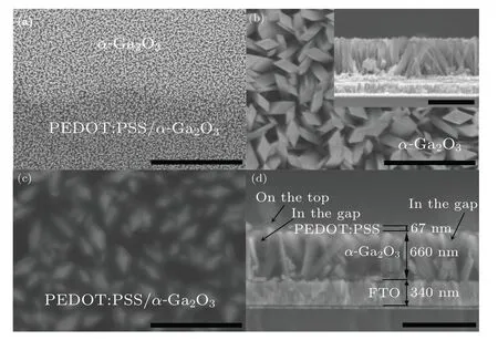
Fig. 1. (a) SEM image of PEDOT:PSS/α-Ga2O3 nanorod array/FTO heterojunction. (b) Surface morphology of the α-Ga2O3 nanorod array. (c)Surface morphology of PEDOTS:PSS-coated α-Ga2O3 nanorod array. (d)Cross section image of PEDOT:PSS/α-Ga2O3 nanorod array/FTO heterojunction. The scale bar in (a) indicates 10 µm. The scale bars in (b)-(d)indicate 1µm.
Figure 2(a) is the XRD patterns of FTO, GaOOH/FTO andα-Ga2O3/FTO. The FTO substrate has seven diffraction peaks of SnO2, corresponding to the crystal faces of (110) at~26.6°,(101)at~33.8°,(200)at~37.9°,(211)at~51.7°,(220) at~54.7°, (310) at~61.7°and (301) at~65.8°(PDF#411445). Besides the FTO peaks,the peaks at~35.4°,~62.6°and~67.1°can be assigned to be (021), (002)and(070)faces diffraction of GaOOH,respectively(PDF#06-0180).Forα-Ga2O3/FTO,the peaks of(110)at~36.2°,(024)at~50.5°,(214)at~63.7°and(300)at~65°correspond to the diffraction ofα-Ga2O3(PDF#06-0503).No other GaOOH diffraction peaks occur inα-Ga2O3/FTO sample,which is further indicative of the total transformation ofα-Ga2O3into GaOOH after GaOOH was annealed at 550°C.Figure 2(b)is the absorption spectra ofα-Ga2O3/FTO and PEDOT:PSS/α-Ga2O3/FTO. Obviously,α-Ga2O3/FTO and PEDOT:PSS/α-Ga2O3/FTO shows the similar absorption properties. Further,the optical bandgap can be roughly estimated by extrapolating the straight-line portion to thehνaxis from the plots of(αhν)2vs.hνin the inset of Fig.2(b). The optical bandgap ofα-Ga2O3is~5.03 eV, which is similar to that of the PEDOT:PSS/α-Ga2O3/FTO(~4.97 eV).

Fig. 2. (a) XRD patterns of FTO, GaOOH/FTO and α-Ga2O3/FTO. (b) UV-vis diffuse reflectance absorption spectra of α-Ga2O3/FTO and PEDOT:PSS/α-Ga2O3/FTO.The inset shows the plots of(αhν)2 vs. hν for α-Ga2O3/FTO and PEDOT:PSS/α-Ga2O3/FTO.
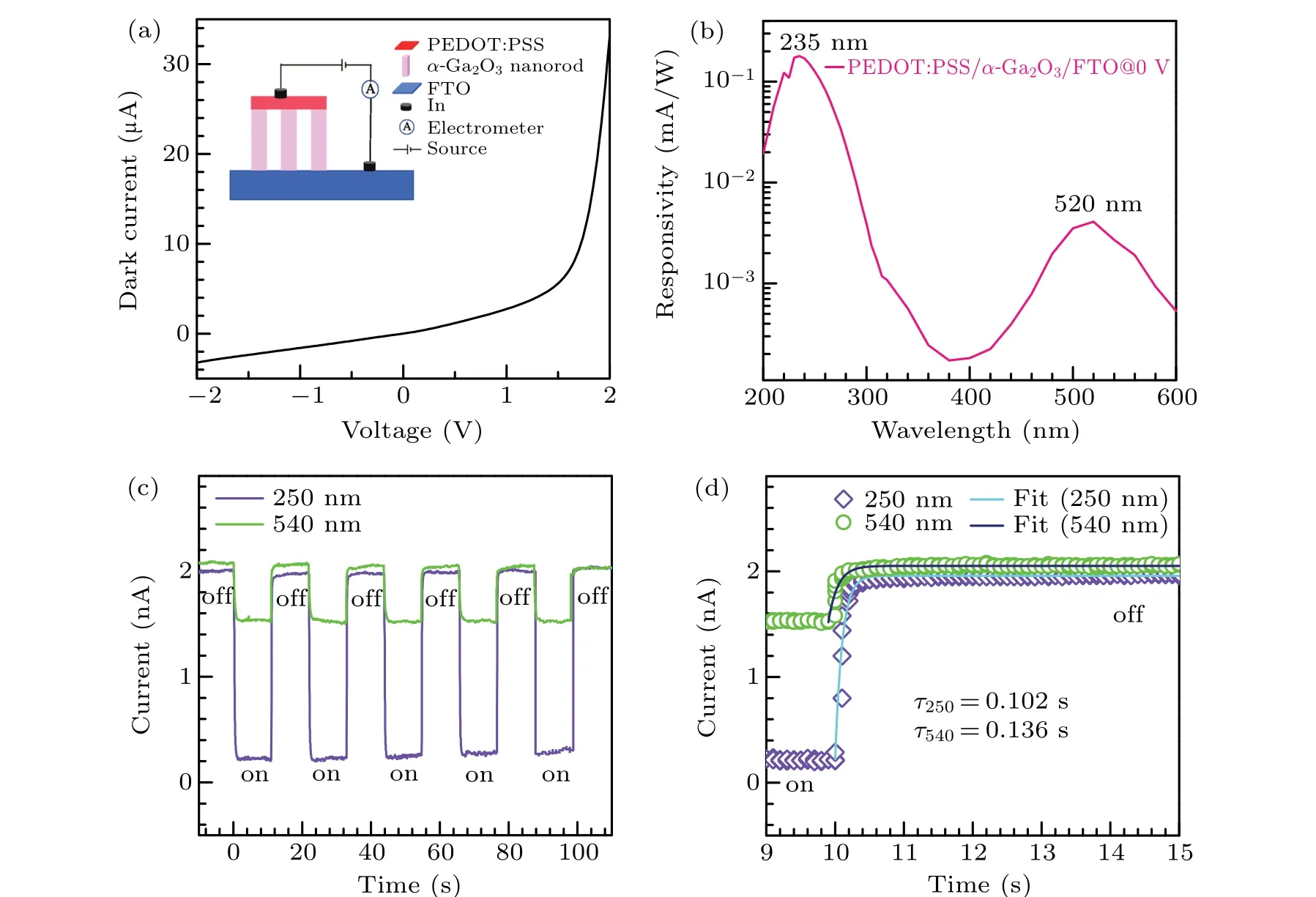
Fig.3. (a)Schematic depict and dark current of PEDOT:PSS/α-Ga2O3 nanorod array/FTO(PGF)device. (b)Responsivity in logarithmic scale of the PGF photodetector at 0 V.(c)Time-dependent current of the PGF device at 0 V under 250 nm(0.23 mW/cm2)and 540 nm(3.31 mW/cm2)with 10 s on and 10 s off. (d)Decay processes of time-dependent current of the PGF device at 0 V under 250 nm(0.23 mW/cm2)and 540 nm(3.31 mW/cm2).
Figure 3(a) schematically shows the illustration of the PGF photodetector. The detailed fabrication processes can be found in the experimental details. The PGF photodetector consists of three parts, including FTO substrate (~340 nm),α-Ga2O3nanorod array (~660 nm) on FTO and the spincoated PEDOT:PSS (~67 nm) onα-Ga2O3nanorod array.In metallic pads were mechanically pressed on PEDOT:PSS and FTO for photoelectric measurements,respectively. When forward voltage is applied to the PEDOT:PSS film, forward current is detected by the electrometer as depicted in Fig.3(a).An obvious rectifying behavior occurred during the dark current measurement. As shown in Fig.3(a),good rectifying heterojunction should contribute to the rectifying property of the dark current. And good rectifying heterojunction is also the foundation of the self-powered photodetection. In Fig. 3(b),the spectral photoresponse at 0 V indicates the capability of self-powered dual-band photodetection. The dominant solarblind UV band centers at 235 nm with a peak responsivity of 0.18 mA/W and a cutoff wavelength of 258 nm. Besides,the other subband photoresponse centering at 520 nm also exists in visible band with a peak responsivity of 0.004 mA/W and a cutoff wavelength of 555 nm. Therefore,a self-powered solarblind UV/visible dual-band photodetection has been successfully realized in our PGF photodetector. Figure 3(c) is the time-dependent current of the PGF device at 0 V under 250 nm(0.23 mW/cm2)and 540 nm(3.31 mW/cm2)with 10 s on and 10 s off, which shows a good stability and repetition in both solar-blind UV and visible bands. As shown in Fig.3(d), the light current decay (I(t)) under 245 nm and 540 nm can be well fitted by the following equation:I(t)=Is+Ie-t/τ(whereIsis the steady current,Iis the photocurrent, andτis the decay time).[3,10]From Fig.3(d),the decay time is 0.102 s under 250 nm and 0.136 s under 540 nm.
Figures 4(a) and 4(b) schematically show the energy band diagrams in theory of the PEDOT:PSS/α-Ga2O3/FTO heterojunction at 0 V under solar-blind UV light and visible light, respectively. As is known, if a heterojunction is formed between p-type PEDOT:PSS and a n-type semiconductor, it can exhibit rectifying property, for example,the PEDOT:PSS/β-Ga2O3heterojunction.[17,18]However,α-Ga2O3nanorod array was fabricated on the FTO substrate through hydrothermal and annealing processes. Therefore,large amounts of interface defects were formed at the interface ofα-Ga2O3/FTO as schematically shown in Figs. 4(a)and 4(b). And, such interface can usually be regarded as ohm-like contact.[17,20]Therefore, rectifying PEDOT:PSS/α-Ga2O3heterojunction in PEDOT:PSS/α-Ga2O3/FTO structure,just like the rectifying PEDOT:PSS/β-Ga2O3heterojunction in PEDOT:PSS/β-Ga2O3/Si structure,results in the rectifying property of the dark current and the self-powered behaviors in the PGF photodetector.[17]To better understand the absorption region of solar-blind UV light, the absorption coefficients of PEDOT:PSS andα-Ga2O3were respectively estimated to be~2.5×104cm-1(250 nm)and~1.2×104cm-1(250 nm) from the data in literature.[25,26]Therefore, the roughly estimated penetration depth of 250 nm light in PEDOT:PSS andα-Ga2O3was about 400 nm and 833 nm, respectively. It should be noteworthy that absorption coefficient will become much larger with increasing the photon energy,which indicates the shorter penetration depth of shorterwavelength solar-blind UV light. Considering the thickness of PEDOT:PSS (~67 nm) andα-Ga2O3(~660 nm), it is deduced that most of the solar-blind UV light can be absorbed in PEDOT:PSS andα-Ga2O3. As shown in Fig. 4(a), photogenerated electron-hole pairs can be separated in the depletion regions of bothα-Ga2O3and PEDOT:PSS under the specific solar-blind UV photons with larger energy than the bandgap ofα-Ga2O3and PEDOT:PSS.Based on the reported self-poweredα-Ga2O3nanorod array/FTO photoelectrochemical cell, it possessed the similar fabrication processes ofα-Ga2O3nanorod array.[23]Therefore, the interface defects ofα-Ga2O3/FTO and bulk defects inα-Ga2O3nanorod array should also be presented in that structure.[23]However,no visible photoresponse was observed.[23]So,we deduce that the interface and bulk defects shows no observable photo-sensitivity to visible light.However,the bandgap of PEDOT:PSS is about 2 eV and a broad band visible absorption can be observed in PEDOT:PSS.[26,27]Therefore, photogenerated carriers can be only generated and separated in the depletion region of PEDOT:PSS under the specific visible photons with larger energy than the bandgap of PEDOT:PSS(Fig.4(b)). When the carries reach theα-Ga2O3/FTO interface,they can also pass through by the assistance of the interface defects as shown in Fig.4.[20]
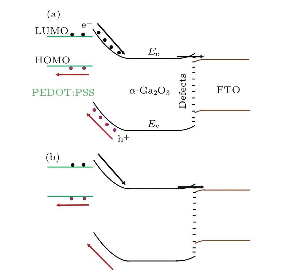
Fig. 4. Energy band diagrams of the PEDOT:PSS/α-Ga2O3/FTO heterojunction at 0 V under solar-blind UV light (a) and visible light (b).LUMO and HOMO respectively present the lowest unoccupied molecular orbital and the highest occupied molecular orbital energy levels of PEDOT:PSS.Ec,Ev,e-and h+donate conduction band,valance band,electrons and holes,respectively. The black and red arrows indicate the directions of electrons and holes transportation at 0 V,respectively.
As shown in Fig.4,the direction of the forward current in our device in Fig.3(a)is just the forward direction in general for Schottky junctions.As is well known,reverse photocurrent will be detected as photocarriers are generated in the depletion region of Schottky junction.Thus,reverse photocurrent in Fig.3(c),the same direction as the dark current under reverse biased voltages,can be observed when electrons and holes are collected by FTO and PEDOT:PSS, respectively. During the self-powered measurements in Fig.3(c),initial dark current is~+2 nA.Owing to the superposition of the dark current and the reverse photocurrent, the light current in Fig. 3(c) varies from~+2 nA to~+0.2 nA after the 250 nm light on and from~+2 nA to~+1.6 nA after the 540 nm light on,which also indicates the respective generation of the photocurrent of~1.8 nA and~0.4 nA.
Table 1 summarizes the structure, detection band, peak responsivity and decay time of the compared photodetectors with our device. Compared with the other self-poweredα-Ga2O3nanorod array photodetectors with the similar hydrothermal fabrication and annealing methods, our device shows comparable solar-blind UV responsivity and much faster response time than most of them.[21-24]However, the featured and distinguished visible photodetection is realized on the basis of PEDOT:PSS/α-Ga2O3heterojunction, showing a peak responsivity of 0.004 mA/W at 520 nm. Besides,the photoresponse speed is much faster than the non-selfpoweredβ-Ga2O3/MoS2/Ce6 DUV/visible dual-band photodetectors due to the fast-speed separation of photogenerated carries by built-in electric field in the depletion regions of PEDOT:PSS/α-Ga2O3heterojunction.[19]Therefore, the fast-speed self-poweredα-Ga2O3solar-blind UV/visible dualband photodetectors can be demonstrated through cheap and simple processes including hydrothermal, annealing and spin coating.
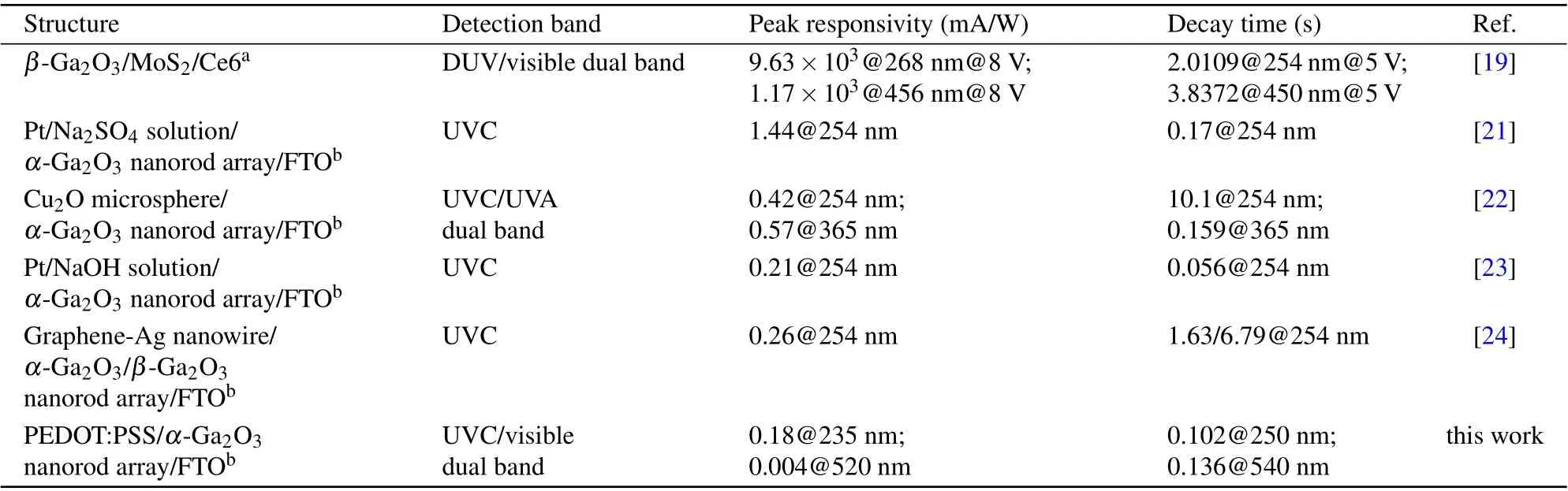
Table 1. Structure,detection band,peak responsivity and decay time of photodetectors.
4. Conclusion
A self-powered PEDOT:PSS/α-Ga2O3nanorod array/FTO solar-blind UV/visible dual-band photodetector has been successfully demonstrated by hydrothermal, annealing and spin coating processes. The photodetector shows comparable solar-blind UV responsivity (0.18 mA/W) and much faster response speed(0.102 s)than most of the self-poweredα-Ga2O3nanorod array solar-blind UV photodetectors. However, it also possesses the featured and distinguished visible band photoresponse with a response speed of 0.136 s at 540 nm. Besides, the response time is much faster than the non-self-poweredβ-Ga2O3/MoS2/Ce6 DUV/visible dualband photodetectors due to the fast-speed separation of photogenerated carries by built-in electric field in the depletion regions of the PEDOT:PSS/α-Ga2O3heterojunction. Therefore, the article herein is anticipated to prove a feasible route toward realizing fast-speed self-poweredα-Ga2O3solar-blind UV/visible dual-band photodetectors by cheap and simple processes for the applications of multiple target tracking,imaging,machine vision and communication.
Acknowledgement
Project supported by the National Natural Science Foundation of China(Grant No.61705155).
- Chinese Physics B的其它文章
- Quantum walk search algorithm for multi-objective searching with iteration auto-controlling on hypercube
- Protecting geometric quantum discord via partially collapsing measurements of two qubits in multiple bosonic reservoirs
- Manipulating vortices in F =2 Bose-Einstein condensates through magnetic field and spin-orbit coupling
- Beating standard quantum limit via two-axis magnetic susceptibility measurement
- Neural-mechanism-driven image block encryption algorithm incorporating a hyperchaotic system and cloud model
- Anti-function solution of uniaxial anisotropic Stoner-Wohlfarth model