
Nonlinear optical properties in n-type quadruple δ-doped GaAs quantum wells
2022-04-12 03:44HumbertoNoverolaGamasLuisManuelGaggeroSagerandOutmaneOubram
Chinese Physics B 2022年4期
Humberto Noverola-Gamas Luis Manuel Gaggero-Sager and Outmane Oubram
1Divisi´on Acad´emica de Ingenier´ıa y Arquitectura,Universidad Ju´arez Aut´onoma de Tabasco,Carretera Cunduac´an-Jalpa de M´endez Km. 1 Col. La Esmeralda,Cunduac´an,8660,M´exico
2Centro de Investigaci´on en Ingenier´ıa y Ciencias Aplicadas,Universidad Aut´onoma del Estado de Morelos,Av. Universidad 1001 Col. Chamilpa,Cuernavaca,62209,M´exico
3Facultad de Ciencias Qu´ımicas e Ingenier´ıa,Universidad Aut´onoma del Estado de Morelos,Av. Universidad 1001 Col. Chamilpa,Cuernavaca,62209,M´exico
Keywords: delta-doping,n-type GaAs layers,electronic structure,non-linear optical properties
1. Introduction
Recently,different approaches allow calculations of optical and electronic properties in semiconductors. For instance,the density functional theory (DFT) can describe accurately the physical properties in multiple materials.[1-5]However,in this method,the calculation time efficiency in the processes is mainly determined by the diagonalization routines.[6]Besides,another approach, the Thomas-Fermi (TF) theory[7,8]allows the determination of the electronic structure with a very simple way in comparison to the DFT.
In the last few years, nano-scale semiconductor devices based on quantum dots, quantum rings, quantum wires and quantum wells have been made possible thanks to the remarkable advances in theoretical investigation.[9-13]Within the TF approach,the electronic structure of quantum wells can be determined. These low-dimensional systems have been widely studied due to their optical and electronic properties.[14,15]A great diversity of structures based on quantum wells are currently being studied, such as materials with epitaxial growth,heterostructures and doped-delta. Aδ-doped quantum well is a two-dimensional layer doping that creates an approximately V-shaped doped potential profile into a structure, where the charge carriers (electrons or holes) form a two-dimensional gas. These systems are very important for the development of optoelectronic devices since its introduction by Wood.[16]
The doping of semiconductor materials in atomic resolution (δ-doping) is possible due to the precision of molecular beam epitaxy (MBE) growth techniques.[17,18]The synthesis ofδ-doped structures has primarily been on gallium arsenide(GaAs). When Si atoms substitute the positions of Ga atoms in the direction (100), a n-type semiconductor[19]is formed .The literature concentrates a lot of information on this material related to subband structure, electron or hole mobilities,and optoelectronic properties.[14,15,20-25]On the other hand,lower number works have been conducted on delta-layers for Si,and this is due to the problems to incorporate dopants in a controlled process of MBE growth for Si.[26]
Another important point is that, inδ-doped potential profiles cases, there are recent studies in nonlinear optical properties.[15,23,27,28]For instance, Durmuslaret al.[20]determined the effects on the nonlinear optical rectification,second harmonic generation,and third harmonic generation of n-type asymmetric double delta-doped GaAs quantum well. In this work,the obtained results indicate that an electric field leads to optical red-shift on nonlinear coefficients while the magnetic field causes optical blue-shift. On the other hand, in the previous work,[29]we represented a model for the n-type quadrupleδ-doped(QDD)system in GaAs. This paper was the first physical model in the literature for the QDD system. Besides,we investigated the electronic structure of QDD in the framework of TF approach. In recent years, some relevant results reported the effects of the external fields such as the magnetic and electric fields,and also the intense laser field. Dakhlaouiet al.[30]investigated the effects of the electric and magnetic field on the linear and nonlinear optical properties of a quantum well heterostructure containing triple parabolic barriers in GaAs. They obtained that an increase in the intensity of the intense laser field produces a shift in the nonlinear optical properties. Our work,shows the effects of internal parameters(interlayer distance and density of impurities)on nonlinear optical properties for quadrupleδ-doped quantum wells.
Up to our knowledge, this work is the first study on nonlinear optical properties in a quadrupleδ-doped structure.Here,we use the framework of the TF approach and the effective mass approximation to obtain the electronic structure of n-type QDD. The determination of nonlinear optical properties is carried out from the density matrix equations. Section 2 shows our methodology, and results and related discussions are presented in Section 3. Section 4 includes the conclusion.
2. Methodology
It was made a theoretical investigation for quadruple ntypeδ-doped GaAs quantum wells (QDDQWs) for different distances between layers (d) and two-dimensional impurities density(N2D). Within the framework of effective mass and TF approaches,the interaction potential between the carriers and the ionized impurity layer in effective units was defined as Equations (3)-(5) and (6)-(7) represent the nonlinear optical properties calculated in this work.


3. Results and discussion


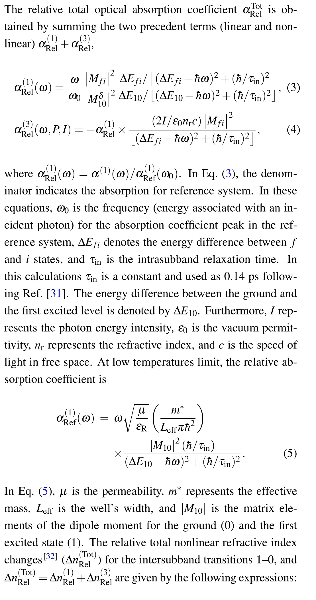
The effect of the interlayer distance of the QW on the electronic structure is shown in Fig. 2. In this figure, it can be observed the reference potential profile and for three different interlayer distances ofd=10 °A, 25 °A and 50 °A, denoted by (b), (c) and (d), respectively. In the cased= 0,corresponding to an insolatedδ-doped quantum well (reference system), we observe the five characteristic levels withN=5×1012cm-2concentration.[33]In order to understand the evolution of the energy levels with the interlayer distance in each of these cases, it is enough to observe the changes at the potential bottom as thedincrease.In these diagrams,it can be observed the geometry change of the potential profile and the increase in the relative maximum atz=0 with the increase of the interlayer distance.

Fig.1. Potential profile,(a)N2D=5×1012 cm-2 and(b)N2D=7.5×1012 cm-2.
Fig.2. Evolution of potential profile, energy, and square of waves functions for(a)reference δ-doped,(b)d1 =10 °A,(c)d2 =25 °A and(d)d3=50 °A.In all cases,the concentration of impurities in the layer is NRef2D =5×1012 cm-2.
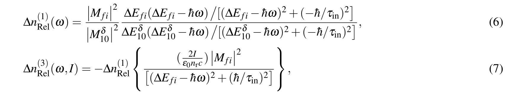
Figure 3 represents the linear, non-linear, and total relative absorption coefficients as a function of the photon energy for four different interlayer distancesd=10 °A, 25 °A, 50 °A and 75 °A. The continuous black line shows the reference absorption coefficient. In this figure, it is possible to observe a red-shift of the total absorption coefficient peak as the interlayer distance is increased. The behavior can be described as follows: by increasingdthe ground state and the first energy level tend to get closer to each other as shown in Figs. 2(b)-2(d). In agreement with Eqs.(3)and(4),the absorption peak reduction by increasingdresults in requiring lower energy of the incident photon to observe the resonant peak,and this implies the red-shift effect. Besides,the above causes a decrease of the amplitude of the absorption resonant peak,which is directly proportional to the frequency of the incident photon energy.
Fig.3. (a)Linear,(b)non-linear and(c)total relative absorption coefficients as a function of the photon energy for four interlayer distances.The different interlayer distances,are considered d=10 °A,25 °A,50 °A and 75 °A.The black dotted line represents the reference system. It was used I=0.1 MW/cm2 for the incident light intensity.
Finally,we plot in Fig.4 the(a)linear,(b)nonlinear and(c) total relative refraction index change as a function of the incident photon energy for different interlayer distance values:d=10 °A, 25 °A, 50 °A, 75 °A. We can be seen a red-shift described on the optical absorption coefficient. This shift is controlled by the variation of the transition energy between the two first energy levels.
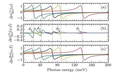
Fig.4.The relative(a)linear,(b)nonlinear and(c)total refractive index changes as a function of the incident photon energy for four different interlayer distances.
It can be observed in the QDD that the absorption coefficient peak is much higher with respect to other structures (single-delta, double delta, heteroestructures) due to the high ΔEbetween the ground state and the first excited state. This condition allows that new optoelectronic devices can be designed based on the QDDQWs structure, such as high-speed electronic-optical modulators, far-infrared photodetectors,and infrared lasers.
4. Conclusions
It was performed a theoretical investigation on the behavior of nonlinear optical properties in a symmetric quadrupleδ-doped quantum well with respect to the interlayer distance.The ground and the first excited state have been considered in order to analyze the optoelectronic properties. The results show that the positions of the resonant peaks of optical absorption coefficient and relative refractive index change versus incident photon energy exhibit a red-shift with an increment of the interlayer distance. The results show the importance that could be tuned by the interlayer distance, the peak locations,and amplitudes of the nonlinear optical coefficients. Finally,the results could be helpful for the studies based on electronic and optical properties in theδ-doped structures.
- Chinese Physics B的其它文章
- Quantum walk search algorithm for multi-objective searching with iteration auto-controlling on hypercube
- Protecting geometric quantum discord via partially collapsing measurements of two qubits in multiple bosonic reservoirs
- Manipulating vortices in F =2 Bose-Einstein condensates through magnetic field and spin-orbit coupling
- Beating standard quantum limit via two-axis magnetic susceptibility measurement
- Neural-mechanism-driven image block encryption algorithm incorporating a hyperchaotic system and cloud model
- Anti-function solution of uniaxial anisotropic Stoner-Wohlfarth model