
Memristor-based multi-synaptic spiking neuron circuit for spiking neural network
2022-04-12 03:44WenwuJiang蒋文武JieLi李杰HongboLiu刘洪波XicongQian钱曦聪YuanGe葛源LidanWang王丽丹andShukaiDuan段书凯
Chinese Physics B 2022年4期
Wenwu Jiang(蒋文武) Jie Li(李杰) Hongbo Liu(刘洪波) Xicong Qian(钱曦聪)Yuan Ge(葛源) Lidan Wang(王丽丹) and Shukai Duan(段书凯)
1College of Artificial Intelligence,Southwest University,Chongqing 400715,China
2National&Local Joint Engineering Laboratory of Intelligent Transmission and Control Technology,Chongqing 400715,China
3Brain-inspired Computing and Intelligent Control of Chongqing Key Laboratory,Chongqing 400715,China
4Chongqing Brain Science Collaborative Innovation Center,Chongqing 400715,China
Keywords: memristor,multi-synaptic circuit,spiking neuron,spiking neural network(SNN)
1. Introduction
In recent years, with the rapid development of artificial intelligence, artificial neural networks (ANNs)have been applied in various fields.[1-4]Spiking neural networks (SNNs)are known as the third generation of the neural network.[5]Neurons transmit information by sending pulse signals to each other, which simulates the information processing model of neurons in the human brain. Compared with the previous two generations,it is more similar to the biological neural network.SNNs have attracted the attention of scholars due to their rich neurodynamic characteristics in the field of space and time,diverse coding mechanisms,and event-driven advantages.[6]
With the continuous development of SNNs,its theory has been very advanced. Many scholars have focused their research on the hardware implementation of SNNs. SNNs emulate the computational paradigm of biological neurons. As the depth of the network increases, the connections between neurons become more complex and the network parameters become larger and larger, which makes the task of implementing artificial neural networks with hardware more difficult. Therefore, building SNNs with hardware to simulate human brain systems requires the use of devices that can be large-scale and high-density integration,low power consumption, and good stability. In 1971, Chua (University of California at Berkeley) pointed out that nature should also exist as one circuit element, it represents the relationship between the magnetic flux and charge.[7]In 2008, HP personnel first discovered nano memristor devices.[8]Memristors are passive devices with nonlinear and non-volatile characteristics. Its resistance is related to the amount of charge passing through it.Due to its nanometer size, it can achieve ultra-high integration and is easy to be controlled. It is perfectly compatible with CMOS technology in the production process.[9]Due to the good characteristics of the memristor, it has been widely used in neural computing, especially as a synapse of neural networks with outstanding performance.[10-14]Because of the similarity between memristors and biological synapses,memristors are widely used in SNNs.For example,Gerardet al.[15]proposed a spiking neuroevolutionary system, which realized memristors as plastic connections. Liuet al.[16]constructed a spiking neural network based on memristor for image edge extraction. Huet al.[17]proposed a memristor-based dynamic(MD)synapse design with memristor models. Zayeret al.[18]present the implementation of low power and ultrafast spiketiming-dependent plasticity(STDP)of the spiking neural network(SNN)in a crossbar structure based on the ferroelectric tunnel memristor (FTM). Zohrehet al.[19]used LIF neurons and memristive synapses to construct a fully connected SNN with 2×2 and 4×2 structures for pattern classification. In these works, memristors are used as synapses of neural networks, demonstrating the value of memristors in neural networks. But these synaptic designs hardly involve discussions about multi-synaptic connections and synaptic signal transmission delay. Therefore, discussing the realization of multiple synapses in hardware circuits has great value and potential.
The design of spiking neurons is also an important part of SNNs. To simulate the working mode of biological neurons,various types of spiking neuron models have been proposed.The first proposed is the Hodgkin-Huxley (HH) model,[20]which is the closest to biological neurons,but the calculation is too complicated and difficult to implement with circuits. Later models such as the Izhikevich model,[21]Leaky integrate-andfire (LIF) model.[22]were proposed. The LIF model is close to real biological neurons, and at the same time, there is no particularly complicated calculation process, and it is widely used in SNNs. On this basis, with the continuous efforts of researchers, various neuron circuits have been proposed one after another.[23,24]For example, Afifiet al.[25]proposed a new CMOS-nano circuit for efficient implementation of spike neurons. Yunuset al.[26]used their proposed memristor to construct a new neuron circuit that can generate spiking and burst to fire behavior.Kimet al.[27]proposed a spike-triggered adaptive neuron circuit with input current modulation. Zhaoet al.[28]designed a new spiking neuron circuit based on the conventional LIF neuron, which uses the nonlinear variation of memristance to generate spikes. Wooet al.[29]proposed an integrate-and-fire (IF) neuron circuit using a single-gated silicon nanowire feedback field-effect transistor that utilizes a positive feedback loop. These works provide many options for the circuit realization of the spiking neuron. However,the design of the spiking neuron circuit with high controllability,good network adaptability,and large-scale integration capability is still the focus of research.
In this paper, firstly, the MSC based on the cross-array of spin memristors is proposed, which simulates the multisynaptic connections between biological neurons. Different strengths of the synaptic connection between neurons can be simulated by setting different weights of memristors in this circuit. By setting different time delays to the delay device, the signal transmission duration of different biological synapses can be simulated. With proper setup,the whole circuit can simulate the multi-synaptic connection between biological neurons and the multi-delay process of information transmission.The synaptic function is realized by the memristor cross-array,which makes the network operation faster,reduces energy consumption,and improves the integration of the network. The MSC is simulated by PSPICE,and the expected simulation results are obtained. Secondly, a spiking neuron circuit based on the LIF model is designed. The neuron circuit can complete the functions of input pulse integration, membrane voltage leakage, and pulse emission. And this circuit can be combined with MSC to form MSSN,which can be used to build SNNs. Compared with previous work,the neuron circuit has the advantages of easier implementation, low device consumption,adjustable pulse threshold,and adjustable pulse width. The PSPICE simulation verifies the feasibility and robustness of the neuron circuit,which can provide more options for the hardware implementation of SNNs. Finally, based on the mathematical model of the MSSN circuit, a small SNN was designed and simulated in Python. The network was applied to classify IRIS-dataset and achieved good classification results.
The following content of this paper is arranged as follows:In Section 2,the memristor used is briefly introduced,and then the MSC based on the memristor cross-array is proposed. In Section 3,a spiking neuron circuit based on the LIF model is introduced. In Section 4,the application of the MSSN circuit model in SNNs is introduced. Finally, Section 5 summarizes the work of this paper and prospects the future work.
2. MSC based on memristors
Simulating biological synapses on hardware has high requirements for the devices used. The size, power consumption, and compatibility of the devices all determine the performance of the synapses. Memristors are nano-scale devices with the characteristics of non-volatility, high scalability, low power consumption,etc., and have a wide range of applications.[30-35]It is a good choice to implement MSC with memristors. The team of Chen from Duke University proposed a spin memristor based on magnetic domain wall movement technology.[36]The spin memristor has good linear characteristics and can meet the requirements of multi-bit data storage. The use of spin memristors in synaptic structures can not only store multi-level synaptic weights but also participate in network calculations. Therefore,the spin memristor is used in the MSC in this paper.
2.1. The MSC
The human brain is a complex, high-density, and extremely low-power information processing system, which contains nearly 1010neurons and 1014synapses.[37]A single neuron can be connected to nearly 104other neurons through synapses.[38]Inspired by biological research,the network structure of multi-synaptic connections was proposed and obtained good results.[39]This multi-synaptic connection strengthens the stability of neural information transmission and storage.[40]Based on this multi-synaptic connection, an equivalent structure based on memristor is proposed as shown in Fig.1. In this structure,two neurons are connected by multiple synapses with different weights and time delays, whereW1,W2,W3,etc. represent the weights of the synapses,which are the resistance values of the corresponding memristors.DelaysD1,D2,D2,etc.control the time delay of the synapse.The synaptic circuit can be used to simulate the connection characteristics between biological neurons.
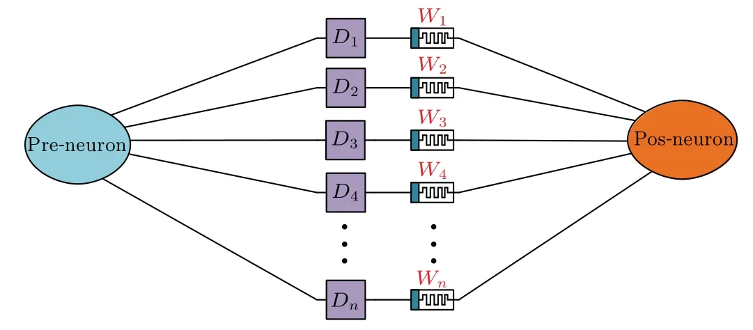
Fig.1. Model of multiple synapses between two neurons. Each synapse is composed of a delayer and a memristor in series. Among them, the resistance value of the memristor represents the synapse weight,and the delayer represents different signal delays.
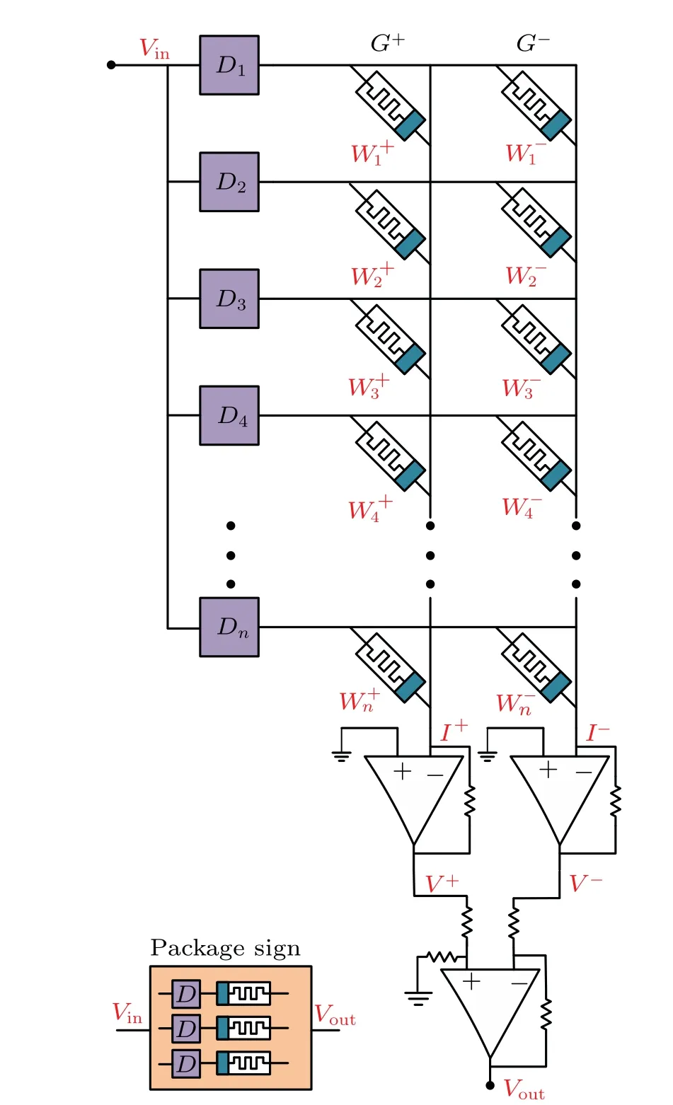
Fig.2. Memristor cross array realizes multi-delay and multi-synaptic connection circuits. Each row of delayers is connected in parallel, and the delayers are connected in series with adjacent memristors. Two memristors connected in parallel represent a weight. After a voltage pulse input, the output voltage Vout of the synapse can be obtained through multi-level calculations.
Arranging the synapse structure on the memristor cross array,the synapse circuit shown in Fig.2 can be obtained. In Fig. 2, the delaysD1,D2,D3,...,Dnare connected to the presynaptic neuron,and each delay is connected in series with the corresponding memristor. The entire memristor cross array realizes multi-synapse and multi-delay synaptic functions.In this circuit, the presynaptic neuron only needs to send one pulse signal to the connected delayer at a time. After the delayer receives the pulse sent by the pre-neuron, it delays the pulse for a preset time, and then transmits the pulse to the memristor connected in series. In this way, it can simulate the multi-delay and multi-synapse connection in SNNs. Due to the existence of inhibitory synapses, their role is to reduce the membrane potential of neurons,so that neurons emit pulses later.In SNNs,negative weights can be used to express this inhibitory effect. Since the resistance values of the memristors are all positive,two memristors in parallel are used to express the positive and negative values of the weights.As you can see in Fig. 2, two rows of memristorsG+andG-are connected in parallel to express weights. The combination of the resistance valuesW+andW-of the two columns of memristors represents one weight. Under the action of the pulse signal,two currentsI+andI-will be generated respectively. At the end of the cross array, these two currents will be converted into voltagesV+andV-,and then through a subtractor to get the final voltageVout, whereVout=V+-V-. The voltage is then output to the postsynaptic neuron to complete the signal transmission task.
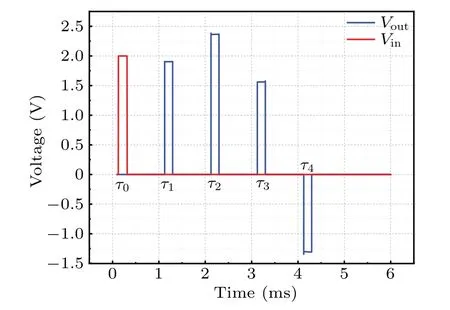
Fig.3. PSPICE simulation results of the MSC.The red line represents the input pulse,and the blue line represents the output result.
This circuit was simulated in PSPICE,and the simulation result is shown in Fig.3. In this simulation,the MSC consists of a 2×4 memristor cross-array is simulated. The resistance values of the columnG+is respectively set to 10 kΩ,12 kΩ,8 kΩ,and 3 kΩ,and the resistance values of the columnG-is all set to 5 kΩ. Meanwhile, each delay device is set to delay 1ms.In the simulation process,a voltageVinis input to the circuit atτ0=0.2 ms,which is a pulse with an amplitude of 2 V.This pulse acts on the memristor atτ1=1.2 ms,τ2=2.2 ms,τ3=3.2 ms, andτ4=4.2 ms after passing through delayersD1~Dn,and generates currentsI+andI+respectively. Then these currents are converted into voltages and subtracted to obtain the final output voltageVout. As can be seen in the figure,the red line represents the input pulse,and the blue line represents the output result. Here are 4 output voltages with different time delays,which are 1.9 V,2.35 V,1.55 V,and-1.3 V respectively,verifying the feasibility of the circuit.
3. Spiking neuron circuit
In the research of simulating biological neurons, various neuron models have been proposed,among which the LIF neuron has been widely used because of its advantages of simple computation and strong mimicry. Based on the LIF model,a new spiking neuron circuit is proposed in this paper. This circuit can integrate the input pulse and continuously leak the voltage when there is no pulse signal input, which simulates the dynamic process of biological neuron signal processing. When the membrane potential of the neuron reaches the threshold, it will send a pulse to the posterior neuron, and at the same time zero its membrane potential. During the period when a spiking neuron emits a pulse, the neuron does not respond to the input pulse until the pulse is emitted. In this spiking neuron circuit,one 555-timer,2-voltage control switches,3-capacitors,and 4 resistors are used. The neuron circuit was simulated by PSPICE, and the expected result was obtained,which verified the feasibility of the circuit.
3.1. Pulse generating module(PGM)
The PGM is an important part of the spiking neuron circuit. In this design, the monostable mode of the 555-timer is used to control the release of pulses.As shown in the blue dotted line on the right side of Fig.4, the 555-timer,R2,R3,R4,S2,C2,andC3form the PGM.In PGM,connect pin 7 and pin 6 of the 555-timer toVCCthrough the upper resistorR3,and then connect to the ground through the capacitorC2. The resistorR3and the capacitorC2are connected in series to control the width of the emitted pulse,andVCCdetermines the amplitude of the pulse. CapacitorC3prevents the 555-timer from being disturbed by noise signals,andR4is a pull-up resistor.
When the amplitude of the input voltageV2of pin 2 of the 555-timer is equal toVCC,the neuron circuit has no output.Only when the voltage amplitude of pin 2 is 0 V,a will pulse be output. The duration of the pulse signal is determined byR3andC2. The duration can be expressed by the following formula:
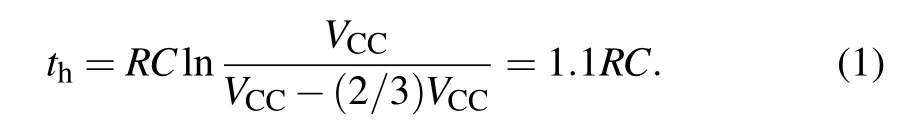
Here,RandCare the values of capacitorC2and resistorR3,respectively, andVCCis the voltage applied to the 555-timer.It can be seen from this formula that the pulse width emitted by the circuit can be adjusted according to requirements. The simulation result of the PGM in PSPICE is shown in Fig.4.
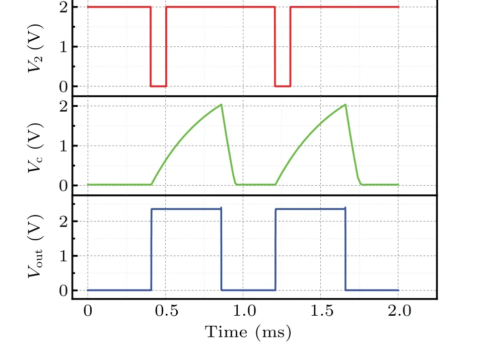
Fig.4. Simulation results of PGM in PSPICE.
3.2. Spiking neuron circuit
The previous chapter briefly introduced the PGM of spiking neurons. Using this module in spiking neurons not only makes the pulse width more controllable but also makes the pulse amplitude more stable. The overall circuit diagram of the spiking neuron is shown in Fig.5.
The red dashed line on the left side of Fig. 5 is the integration and leakage module (ILM) of the spiking neuron.The ILM is composed of a capacitorC1, a resistorR1, and a voltage-controlled switchS1. In this module, the resistorR1is connected in parallel with the capacitorC1, the controlled terminal of the switchS1is connected to both ends ofC1,and the controlling terminal of the switchS1is connected and controlled by the output terminal of the 555-timer. The conduction state of the switchS1determines whether the capacitorC1responds to the input pulse. When the switchS1is non-conducting, the capacitorC1integrates the input pulse and completes the voltage leakage process when there is no input pulse. When the switchS1is conducting, the capacitorC1quickly discharges, and its voltage is set to zero. The capacitorC1can continue to charge until the switchS1is nonconducting.
The purple dashed line in the middle of Fig.5 is the pulse control module (PCM). The control terminal of the switchS2in the module is connected to both ends of the capacitorC1, and the voltage ofC1controls the conduction state of the switchS2. The conduction state of the switchS2determines the 2-pin input of the 555-timer. When the switchS2is nonconducting, pin 2 is equivalent to directly connected toVCCthrough the resistorR2, and the input voltageV2of pin 2 isVCC. WhenS2is conducting, pin 2 is equivalent to directly connected to GND. At this time, the input voltageV2of pin 2 is 0 V,andR2protects the power supplyVCC. The PGM is followed by the pulse control module and is controlled by it.
When a pulse arrives,the pulse will charge the capacitorC1. If the voltageVCof the capacitorC1does not reach the conduction value of the switchS1(the threshold value of the spiking neuron),the spiking neuron does not emit a pulse.And when there is no input pulse,the capacitorC1slowly leaks the voltage through the parallel resistorR1and waits for the arrival of other pulses. If the voltageVCof the capacitorC1gradually increases to be equal to the threshold of the switchS2,the controlled end of the switchS2will be turned on,and the voltage of pin 2 will be pulled down to 0 V.When it happens,the 555-timer starts to work and emits out a fixed-width pulse. And turn on the switchS2through the feedback loop,make the capacitor discharge rapidly. During the pulse emitting process,C1will not be able to charge until the pulse is emitted. This circuit completes the integration,leakage,and firing functions of spiking neurons. The dynamic process of the neuron circuit can be expressed by the following formula:
When there is a pulse input
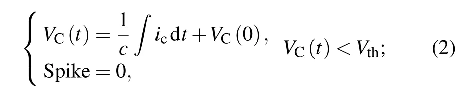
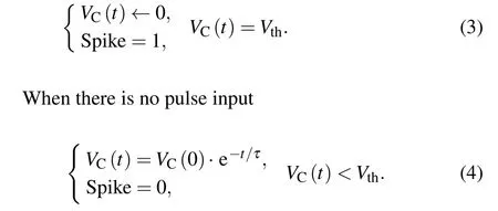
Here,VC(t)represents the membrane voltage of the spiking neuron at timet, andicrepresents the current flowing through the capacitor when the capacitor is charged.VC(0)represents the voltage of the neuron at the last moment. Spike indicates whether a pulsed neuron emits a pulse. When spike is equal to 1,a pulse is emitted,and when spike is equal to 0,no pulse is emitted.τis the time constant,and its value is determined by the capacitorC2and the resistorR3.Vthrepresents the threshold voltage of the spiking neuron.
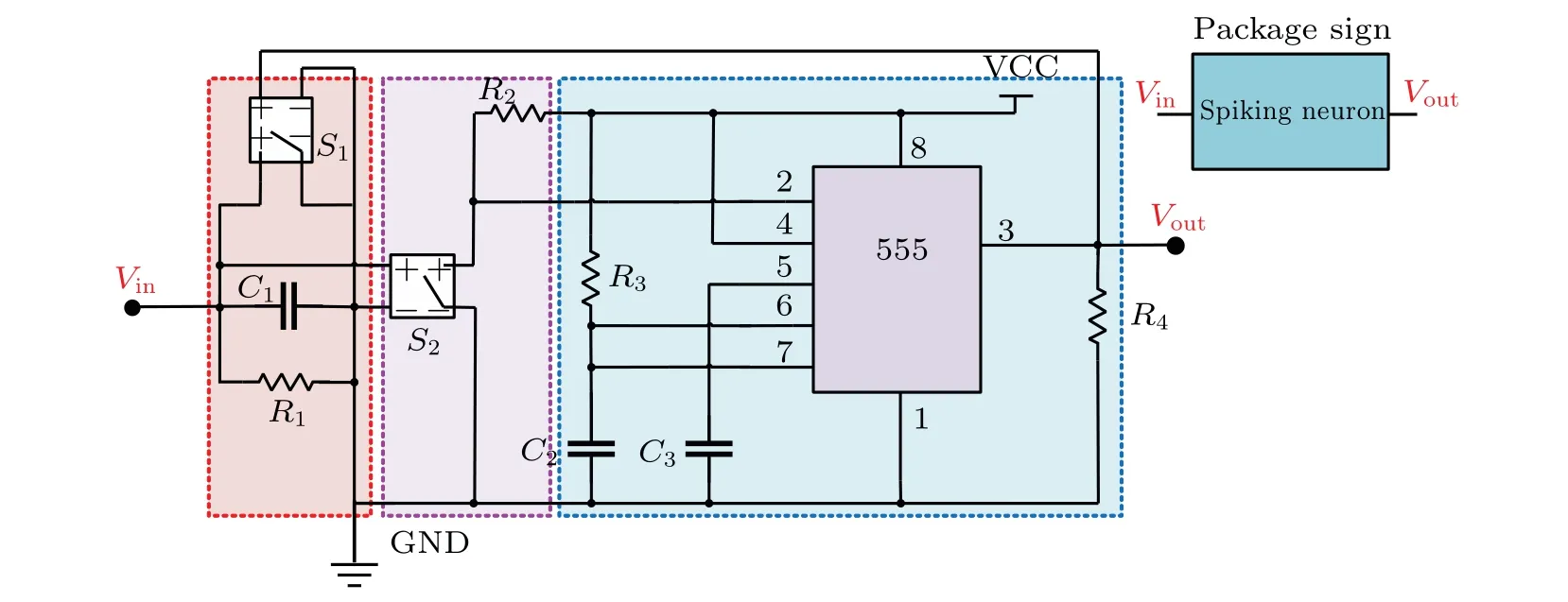
Fig.5. LIF neuron circuit. The red dashed line on the left is the ILM,the purple dashed line in the middle is the PCM,and the blue dashed line on the right is the PGM.

Fig.6. Neuron simulation results in PSPICE. The membrane voltage VC of the spiking neuron gradually increases under the action of the input pulse.When the threshold is reached,a pulse is emitted and the membrane voltage is set to zero.
The spiking neuron circuit was simulated in PSPICE,and the simulation result is shown in Figs.6 and 7.In these figures,Vpulserepresents the pulse input from the pre-neuron,VCrepresents the voltage of the capacitorC1(that is the membrane voltage),andVoutrepresents the pulse firing of the neuron. In the simulation, the threshold of the spiking neuron is set to 1.2 V. In Fig. 6, the neuron receives 4 pulses from the preneuron,and the voltageVCofC1gradually raises with time. It can be seen that the voltageVCleaks over time during the interval between the two pulses. Due to the large amplitude of the 4 input pulses,VCis charged to the threshold at the end of the 4th pulse,and the spiking neuron emits a pulse at this time. In Fig.7,since the amplitude of these 4 pulse inputs is small,theVCcannot be charged to the threshold value,so no pulse is sent out. The simulation verifies the feasibility of the circuit. Compared with the existing spiking neuron circuits,this neuron is more suitable for building SNNs. The threshold value of the neuron circuit,the width,and the amplitude of the firing pulse can be adjusted by the circuit parameters. The initial membrane voltage of the neuron circuit is set to zero instead of a negative voltage,which saves energy consumption and is more suitable for SNN circuit implementation. The circuit also has the advantages of being easier to implement,and low in device and power consumption. At the same time,the neuron circuit can also be combined with the MSC we designed to form the MSSN circuit. The circuit verified the feasibility and robustness of the circuit through PSPICE simulation and provided more options for the hardware implementation of SNNs.
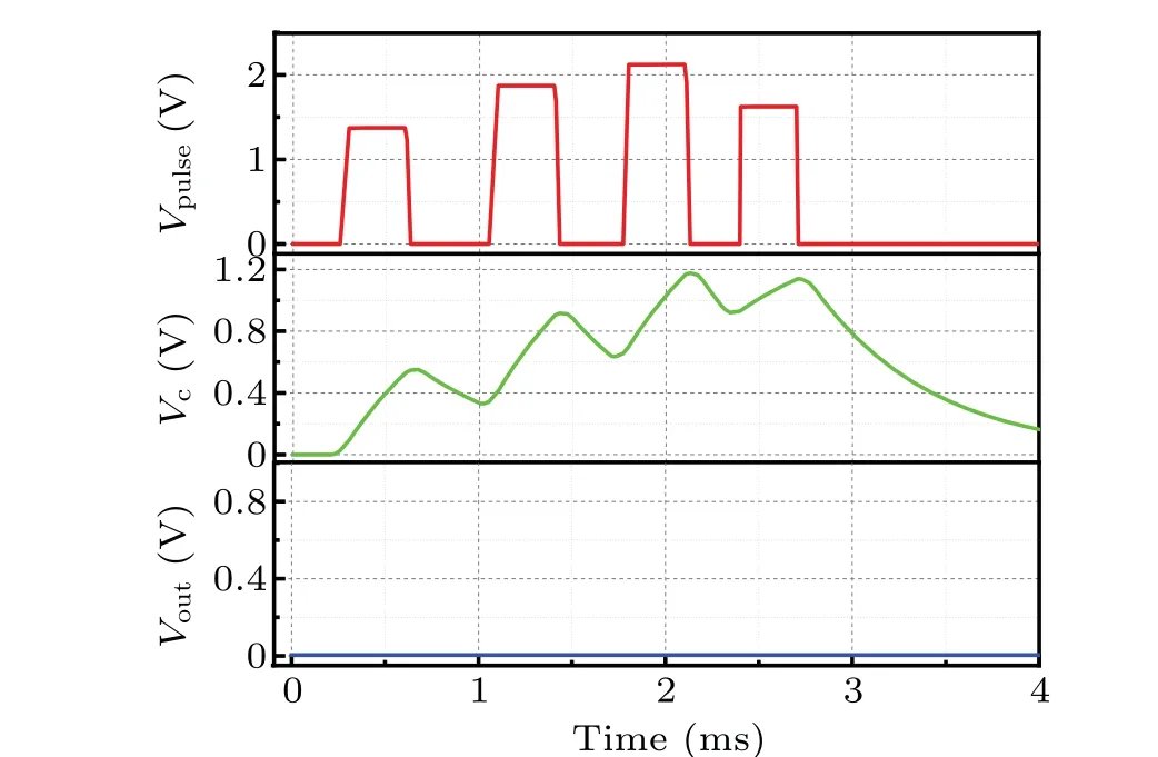
Fig.7. Neuron simulation results in PSPICE.The membrane voltage VC of the spiking neuron gradually increases under the action of the input pulse.However, the capacitor C1 has not reached the threshold, there is no pulse emission and the voltage VC of the capacitor C1 gradually leaks.
3.3. The MSSN circuit
In the second chapter,the MSC with multiple delay functions is introduced,which can convert a single input pulse into multiple delayed pulses and output them. Combine MSC with the spiking neuron circuit to form the MSSN circuit. In theory, a certain number of MSSN circuits can be used to build an SNN with certain functions. The MSSN circuit can be represented in Fig. 8. In Fig. 8, the previously defined package sign is used to represent the corresponding circuit. It can be seen that the MSC and the spike neuron circuit are connected in series to form the MSSN circuit, that is, the output of the MSC is used as the input of the spike neuron circuit.
Fig. 8. MSSN circuit. The circuit consists of a cascade of multi-synaptic circuits and spike neuron circuits.
4. Application in SNN
In this paper,a small SNN is designed to verify the feasibility of the MSSN.Based on the mathematical model of the circuit, a two-layer SNN is built in python, and the SNN is used to classify the IRIS-dataset. Theoretically, SNN based on MSSN circuit design can perform classification tasks on different data sets. By setting the appropriate number of neurons and parameters,with excellent algorithms,it is possible to classify other data types similar to IRIS-dataset,such as Wisconsin Breast Cancer Dataset and Statlog (Landsat Satellite)Dataset. For other larger data sets or data types that are not similar to IRIS-dataset,only after proper preprocessing of the data set and the use of better algorithms, the SNN designed based on MSSN can complete the classification task of the processed data. After training and adjusting the parameters of the network, a good result was finally obtained in the classification task of IRIS-dataset, which verified the feasibility of our design.
4.1. Introduction to IRIS-dataset
IRIS-dataset is a commonly used classification experiment data set. Iris is also called the iris flower dataset,which is a type of data set for multivariate analysis. The data set contains a total of 150 data samples,which are divided into 3 categories,namely,Setosa,Versicolour,and Virginica. There are 50 data in each category, and each data contains 4 attributes.Through the four attributes of calyx length,calyx width,petal length, and petal width, it is possible to predict which of the three types of Iris flowers belong. The 150 samples are divided into two equal parts, one is used as the training set of SNN,and the other is used as the test set of the network.
4.2. Design of the SNN
Based on the MSSN circuit, the circuit can be mapped to the corresponding theoretical model. In a spiking neural network, each spiking neuron is connected toΓjpre-neurons and each connection contains m delay synapses, then neuronjwill receive a set of pulses at the timeti, wherei ∈Γj. The relationship between the state variablexj(t)of the membrane voltage at the peak of neuronjand the input received from all pre-neurons is as follows:[41]
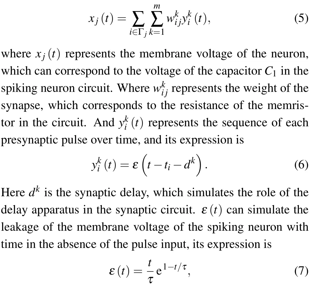
whereτis the time constant, which determines the leakage rate of the neuron membrane voltage,and its value can be determined byR3andC2in the neuron circuit.
According to this mapping relationship, an SNN with a structure of 4×8×1 is built. It includes 4 input neurons, 8 hidden neurons,and 1 output neuron. Neurons are connected by 5 synapses,and each synapse is set with a fixed time delay.The SNN structure contains a total of 40 groups of 5×2 memristor cross arrays, sharing 400 memristors. The structure of the SNN is shown in Fig.9. It can be seen from the figure that 4 input neurons are connected to 8 hidden neurons, and the hidden neurons are connected to output neurons. The contents of the two dashed boxes on the upper right of Fig. 9 indicate that the model of the LIF neuron and synapse in the network structure is consistent with the designed circuits.
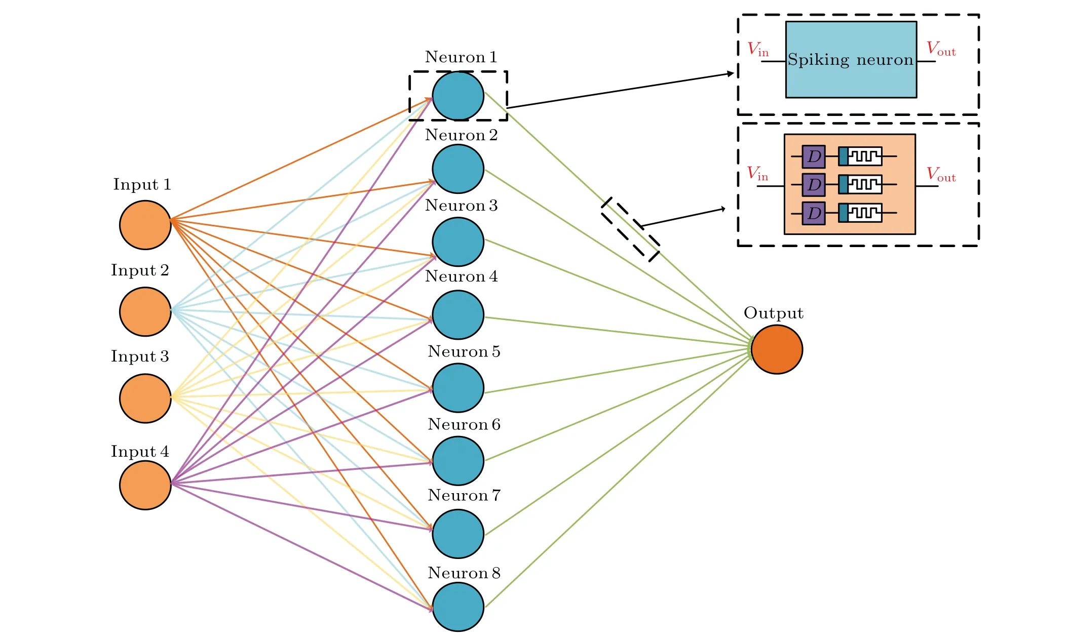
Fig. 9. SNN structure diagram. The structure of SNN is 4×8×1, including 4 input neurons, 8 hidden neurons, and 1 output neuron. Neurons are connected through multiple synapses. The neuron model and synapse model of SNN are consistent with the designed circuits.
4.3. Process and result analysis of SNN
To enable SNN to complete complex recognition tasks,the SpikeProp[41]algorithm is used to train the SNN. During training,the value of each attribute of the sample is used as the pulse input time. For example,when the value of a certain attribute is 3.0 cm,a pulse is input to the corresponding neuron at 3.0 ms. After the network training is completed,the identification accuracy of the network is verified by using the data of the test set. In this SNN,the final result of classification is determined by the time interval of the pulse emitted by the spiking neuron in the output layer. After multiple debugging, the time interval of Setosa class pulse was set at 9.7 ms~10.8 ms,Versicolor class pulse was set at 10.7 ms~11.8 ms, and Virginica class pulse was set at 11.7 ms~12.8 ms. The time here refers to the step size of software iteration calculation,not the real time.
To demonstrate the implementation process of the network,a sample belonging to the Virginica class in the test set is taken out and analyzed separately. The four attributes of this sample are calyx length, calyx width, petal length, and petal width,respectively,6.6 cm,3.0 cm,4.4 cm,and 1.4 cm. The value of the sample data is used as the pulse input time. After the iteration of the network,the pulse output time of the 8 neurons in the hidden layer is 7.69 ms,7.99 ms,7.89 ms,7.99 ms,8.09 ms,8.09 ms,8.09 ms,7.89 ms. Finally,the neuron in the output layer has a pulse time of 12.39 ms. The time 12.39 ms was within the classification interval of 11.7 ms~12.8 ms,and the sample was successfully classified as Virginica. The classification process is shown in Fig. 10. You can see the input time of the pulse and the time each neuron emits the pulse in the figure. The red box at the bottom right of the figure shows that the input pulse at 1.4 ms produces multiple delay pulses after passing MSC.In the figure, only one multi-synaptic delay transmission is drawn,and the other synapses are also analyzed in the same way.
The final classification results on the complete test set are shown in Fig.11. As can be seen from the figure,spiking time is divided into three regions. The orange area at the bottom represents the first class (Setosa), the pink area in the middle represents the second class(Versicolor),and the light blue area at the top represents the third class(Virginica). In the figure,the shape of the red dots represents the sample of Setosa,the shape of the purple triangle represents the sample of Versicolor,and the shape of the blue diamond represents the sample of Virginica. It can be seen from the figure that almost all the samples are within the corresponding time interval, and the identification accuracy reaches 97.33%. The results show that the network can accurately classify and identify the samples in the test set,which verifies the feasibility of the design.
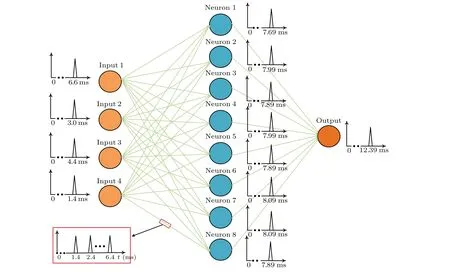
Fig. 10. The process of SNN processing a single sample. The 4 pulses on the left in the figure are the input of the input neuron, which are input at the time of 5.5 ms,3.5 ms,1.3 ms,and 0.2 ms respectively. The 8 neurons in the hidden layer reach the neuron threshold and emit pulses at 6.99 ms,7.59 ms,7.09 ms,7.19 ms,7.49 ms,7.09 ms,6.99 ms,and 7.29 ms respectively. The last output neuron emits a pulse at time 12.39 ms. The red box shows the delayed pulse of the synapse.
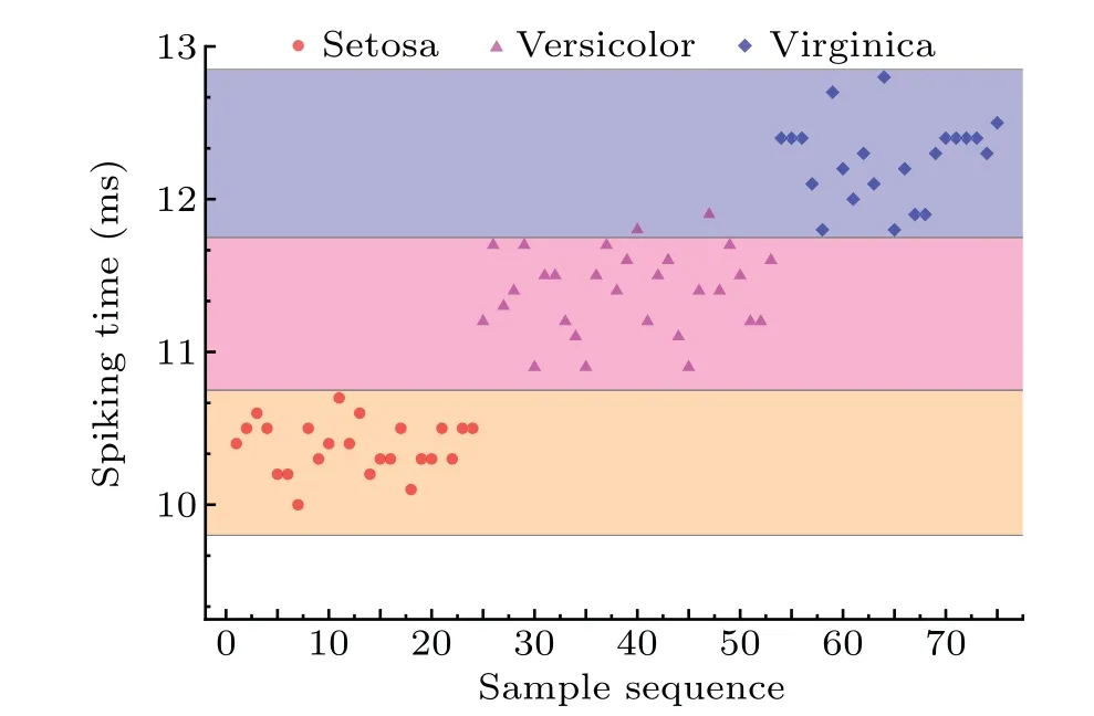
Fig.11. The recognition result of SNN on the test set. The spiking time is divided into three areas, which represent the classification range of different flowers. Circles,triangles,and diamonds represent the samples of three kinds of flowers.
5. Conclusion
In this paper, a memristor-based MSC is designed. This circuit simulates the multi-synapses and multi-delay characteristics of biological neurons. Because memristors are compatible with CMOS technology and have the characteristics of nanometer size, applying the synaptic circuit to the hardware constituting SNNs can save design cost and space. Secondly,a spiking neuron circuit based on the LIF neuron model is proposed. The neuron circuit uses fewer devices and is easy to implement in hardware. The threshold value,pulse width,and amplitude of the neuron circuit can be adjusted by the parameters of the circuit, and the firing pulse is stable. Setting the initial voltage of the neuron circuit to zero not only reduces energy consumption but is more suitable for building SNN circuits. The simulation of PSPICE verifies the controllability and robustness of the neuron circuit. The neuron circuit and MSC can be combined to form MSSN,which can be used to build SNNs. At the end of the paper,the application of MSSN in SNN was simulated based on the theoretical model of the MSSN circuit, and good results were obtained. In the future,we will continue to study the implementation of deep neural networks on hardware to achieve more complex neural networks with less hardware consumption. Provide more choices for the realization of neural networks on hardware.
Acknowledgements
Project supported by the National Key Research and Development Program of China(Grant No.2018YFB1306600),the National Natural Science Foundation of China (Grant Nos.62076207,62076208,and U20A20227),and the Science and Technology Plan Program of Yubei District of Chongqing(Grant No.2021-17).
猜你喜欢
Chinese Physics B(2022年11期)2022-11-21
小小说月刊·下半月(2022年7期)2022-07-19
小小说月刊(2022年14期)2022-07-18
客联(2022年3期)2022-05-31
源流(2021年11期)2021-03-25
小天使·一年级语数英综合(2020年3期)2020-12-16
小天使·一年级语数英综合(2020年2期)2020-02-04
新高考·高二数学(2016年7期)2017-01-23
短篇小说(2014年11期)2014-02-27
故事林(2010年6期)2010-05-14

- Chinese Physics B的其它文章
- Quantum walk search algorithm for multi-objective searching with iteration auto-controlling on hypercube
- Protecting geometric quantum discord via partially collapsing measurements of two qubits in multiple bosonic reservoirs
- Manipulating vortices in F =2 Bose-Einstein condensates through magnetic field and spin-orbit coupling
- Beating standard quantum limit via two-axis magnetic susceptibility measurement
- Neural-mechanism-driven image block encryption algorithm incorporating a hyperchaotic system and cloud model
- Anti-function solution of uniaxial anisotropic Stoner-Wohlfarth model