
Broadband chirped InAs quantum-dot superluminescent diodes with a small spectral dip of 0.2 dB
2022-09-24 08:03HongWang王虹ZunrenLv吕尊仁ShuaiWang汪帅HaomiaoWang王浩淼HongyuChai柴宏宇XiaoguangYang杨晓光LeiMeng孟磊ChenJi吉晨andTaoYang杨涛
Chinese Physics B 2022年9期
关键词:杨涛
Hong Wang(王虹) Zunren Lv(吕尊仁) Shuai Wang(汪帅) Haomiao Wang(王浩淼)Hongyu Chai(柴宏宇) Xiaoguang Yang(杨晓光) Lei Meng(孟磊)Chen Ji(吉晨) and Tao Yang(杨涛)
1Key Laboratory of Semiconductor Materials Science,Institute of Semiconductors,Chinese Academy of Sciences,Beijing 100083,China
2Center of Materials Science and Optoelectronics Engineering,University of Chinese Academy of Sciences,Beijing 100049,China
3College of Information Science and Electronic Engineering,Zhejiang University,Hangzhou 310027,China
4Zhejiang Laboratory,Hangzhou 310027,China
Keywords: chirped quantum-dot,superluminescent diodes,direct Si doping
1. Introduction
A superluminescent diode (SLD) is an ideal optical broadband source for applications such as fiber optic gyroscopes (FOGs), wavelength-division multiplexing (WDM)and optical coherence tomography(OCT).[1-4]The SLD emitting at 1.3 µm is very important for OCT because it has the lowest absorption in human tissue.Resolution is the key to the imaging quality of OCT.The longitudinal resolution is determined by the coherence length(Lc)of the light source,which is related to the spectral width(Δλ)and center wavelength(λ0)byLc≈λ20/Δλ.[3]A wider spectral width can raise the resolution of the OCT.Moreover,a higher output power can improve the sensitivity of the system.[5]Therefore, a simultaneous increase in the output power and spectral width of the SLDs is highly desirable. In addition,the spectral dip is also an important parameter for SLDs,it refers to the value of the depression in the center of spectrum,which represents the flatness of the top of the spectrum.[6]Spectral dip can cause side lobes of the main peak in the point spread function (PSF) of the light source, which can cause noise in the OCT image and reduce the axial resolution.[3]Therefore, post-growth annealing process and optimization of chirped quantum dot(QD)structure are used to obtain the spectrum with flat top.[7,8]
The application of QDs in the active region of SLDs has aroused great interest since it was first proposed, especially for InAs/GaAs QDs.[9-14]Due to the feature of self-assembled QDs grown by Stranski-Krastanow mode,they typically have a large size fluctuation and a Gaussian emission spectrum close to ideal. In addition, owing to the limited density of states for the ground state (GS) of the QDs, the emission of higher excited states(ESs)of the QDs can be easily achieved at a relatively small injection current density,leading to a broadened emission spectrum due to the simultaneous contribution of GS and ESs of QDs. Moreover, to further increase the spectral width of QD-SLDs, a chirped multilayer QD structure of the active region is commonly adopted by depositing strain-reducing layer(SRL)of different thicknesses.[15,16]Majid reported the spectrum dip from the central wavelength of 0.2 dB over 40-nm spans and that<1.5 dB over 300-nm spans for QD-SLDs with the InAs/InGaAs dot-in-a-well (DWELL)structure.[17]Recently, we reported that the spectrum dip is 1.2 dB for InAs/GaAs QD-SLD with direct Si doping in QDs when the spectral width was 105 nm.[18]For QD-SLDs with a central wavelength in the O-band, and utilizing the common contribution of GS and ES to broaden the spectrum,their spectrum dip is not less than 0.2 dB.[19-21]In addition, it is found that doping technology is often used to improve the performance of QD-SLDs, such as p-type modulation doping technology.[22]However, it can only increase the output power, but not broaden the spectrum. Another doping technology is direct Si doping technology.[23]It has been shown that direct Si doping can effectively enhance the performances of QD devices,such as lasers and solar cells.[24,25]Especially,it has been demonstrated that Si doping technology can simultaneously improve the output power and spectral width of QDSLDs.[18]
In this paper, we demonstrated enhanced performances of InAs/GaAs chirped multilayer quantum-dot superluminescent diodes (CMQD-SLDs) with direct Si doping compared with ones without any doping in QDs. It was found that the output power of the doped CMQD-SLD is always higher than that of the undoped CMQD-SLD at identical injection currents. The maximum output power of the doped CMQDSLD reached 1.16 mW at 430 mA,while that of the undoped CMQD-SLD was only 0.06 mW at 290 mA, an increase of approximately 18.3%. The broadest half-maximum full width(FWHM)of the spectrum for the doped CMQD-SLD is 98 nm,compared to only 70 nm for the undoped CMQD-SLD,an increase of approximately 40%. Moreover, the spectral dip of the doped CMQD-SLD is decreased to 0.2 dB, which is the same as the minimum reported for QD-SLDs with a central wavelength in the O-band.[17-21]The improved performance of doped CMQD-SLD can be attributed to the direct doping of Si in the QDs, which passivates the nonradiative recombination centers within or near the QDs and provides excess carriers to occupy the higher excited states.[18,23-25]A shorter cavity length CMQD-SLD was also fabricated, and a maximum spectral width of 106 nm was obtained. In addition, through anti-reflection coating and device packing,the maximum output power and spectral width of CMQD-SLD with direct Si doping were increased to 16.6 mW and 114 nm,respectively.
2. Experiment
The InAs/GaAs CMQD-SLD samples used in the study were grown on n+GaAs(100)substrates by molecular beam epitaxy(MBE).The active region of the CMQD-SLD samples consists of ten stacked layers of~2.2 monolayers InAs QDs with or without Si doping. Each InAs QD layer was capped with an In0.17Ga0.83As SRL and a subsequent 40-nm-thick GaAs barrier layer after the QD layer was deposited. SRLs of different thicknesses were used to realize sequential shifts in the emission center wavelength of the QD layers. The Si atom doping concentration of the InAs QDs in the active region for the doped CMQD-SLD samples was 5×1017cm-3. Both the doped and undoped CMQD-SLD samples contain an n+-GaAs buffer layer, an n-Al0.4Ga0.6As lower-cladding layer, a GaAs lower-waveguide layer, an active region, an upper-waveguide layer, a p-Al0.4Ga0.6As upper-cladding layer, and a p+-GaAs contact layer. The devices were fabricated by standard photolithography,dry etching,contact metallization,and cleaving techniques. The width of the waveguide was 5µm. The“J”-shape ridge waveguide structure was used in this study,which was divided into two parts,one part was a straight waveguide,and the other part was a bent waveguide. We firstly fabricated devices with a cavity length of 3 mm(L=3 mm),with a bending region of 1 mm and a straight region of 2 mm. Next, to optimize the performance of the device, we also fabricated devices with the cavity length of 2 mm (L=2 mm), with a bending region of 1 mm and a straight region of 1 mm. To minimize the optical transmission losses,the curvature radius of the curved area was 0.8 cm.The bent region was tilted from the normal direction of the cleaved facet by 7°.
3. Results and discussion
Figures 1(a)and 1(b)show the power-dependent photoluminescence(PL)spectra of the active regions of the undoped and doped CMQD samples at room temperature (RT). One emission peak of 1289 nm is observed in Fig.1(a),so that the light emission of the undoped sample is mainly from the GSs of the QDs. As the pump power increased,the peak intensity of the PL spectra gradually increased, but the GS peak was always dominant. As the pump power was 5P0(P0=1 W),the FWHM of the PL spectra was only 154 nm. However,two emission peaks at 1203 nm and 1281 nm are observed in Fig.1(b).
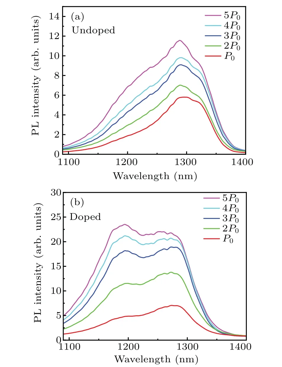
Fig.1. PL spectra from the active region of the doped(a)and undoped(b)samples at RT.
The broad Gaussian-like emission at 1281 nm corresponds to the GS emission of QDs, while the combination of the emission at 1203 nm is the ES emission. As the pump power increased,the energy levels of ES were gradually filled,and the peak intensity of the ES gradually increased, and finally exceeded the peak intensity of the GS,while the FWHM of the PL spectra gradually increased. When the pump power was 5P0, the FWHM of the PL spectra was 175 nm. The broadened PL spectra for the doped sample is attributed to the direct Si doping providing excess electrons, which can lead to an increase in ES emission. It can be easily found from Fig. 1 that the peak intensity of the doped sample is approximately 2.03 times higher than that of the undoped sample at RT. This can be attributed to the fact that Si doping can inactivate the nonradiative recombination centers near or within the QDs and provide excess electrons to fill into higher energy levels,thereby effectively suppressing the nonradiative recombination process.[23]
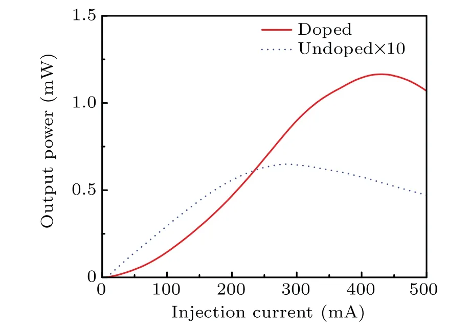
Fig.2. The P-I characteristics of the doped and undoped CMQD-SLDs measured at RT under CW.
Figure 2 shows theP-Icharacteristics of the Si-doped and undoped CMQD-SLDs(L=3 mm)measured under continuous wave(CW)operation at RT.The original output power of the undoped sample is multiplied by ten and plotted in the graph. The cavity facet of the bent waveguide is defined as the front facet of the output. As shown in Fig.2,the CMQDSLDs have typicalP-Icharacteristics,whereP-Ishows a superlinear relationship. TheP-Icurve shows no knee,indicating the suppression of lasing. Furthermore, it can be clearly seen that the output power of Si-doped CMQD-SLD is always higher than that of undoped CMQD-SLD under the same injection currents. This shows that the doped sample has lower output power consumption at the same injection current. In particular,the maximum output power of the Si-doped sample reaches 1.16 mW at 430 mA,while that of the undoped sample is only 0.06 mW at 290 mA.The increase in output power of the doped sample can be attributed to the fact that Si doping can inactivate nonradiative recombination centers near or within QDs,thereby effectively inhibiting the nonradiative recombination process.[23]As the injection current increases,the output power of the CMQD-SLDs reaches a maximum value and then begins to decrease due to the carrier thermal escape at higher injection currents.
Figure 3 presents the optical spectra of the undoped and doped CMQD-SLDs measured at RT. The optical spectra of undoped CMQD-SLD are shown in Fig. 3(a). As the injection current increases, carriers fill higher energy levels, and the center wavelength of the optical spectra gradually shifts to blue and then to red. There is also a gradual increase in the FWHM of the spectrum. The broadest FWHM of spectrum is 70 nm at 500 mA.Additionally,at higher injection currents,the self-heating of the device becomes apparent,and the output power no longer increases.All spectra show a Gaussian shape,and there do not change significantly with increasing injection current. It can be inferred from the central wavelength position of the spectra that the carriers are mainly filled with the GSs of the QDs,so the optical emission of the undoped sample mainly originates from the GSs of the QDs. The optical spectra of doped CMQD-SLD are shown in Fig. 3(b). When the injection current is small, the carriers are randomly filled into each QD in the active region, and preferentially recombine in QDs with a larger size and lower energy level. In this case, the device has a long luminescence wavelength and the device’s luminescence comes mainly from the contribution of spontaneous emission, with a large spectral width. With increasing injection current, the carriers fill into the small and high-energy QDs,and the luminous wavelength of the device is blue shifted. When the peak intensity from the ES of the QDs is equal to that from the GS of the QDs (GS=ES), the spectral FWHM is the broadest. When the injection current is 200 mA, the doped sample achieves the GS=ES regime,and the spectral FWHM is 98 nm. At the maximum spectral FWHM,the output power of the doped sample is 0.5 mW.As the injection current is further increased, the peak of the ES dominates,while the spectral width seems to decrease rapidly due to the significant increase in the contribution of stimulated emission. Since direct Si doping provides excess electrons,more carriers would fill into the ESs of the QDs,and the doped sample achieves the GS=ES regime. For the undoped sample,the GS peak always dominates,and the ES of QDs can not emit. However, the obvious advantage of SLDs with QDs as the active region is to use the common contribution of GS and ES to broaden the optical spectrum. Direct doping with Si enhances the exploitation of this advantage. When the FWHM of the spectrum is at its broadest, the spectrum dip over this range is<0.2 dB, which is smaller than that of the uniform multilayer QD-SLD.[18]Figure 3(c)shows the corresponding change in the FWHM of undoped and doped CMQD-SLD as the injection current increases. The spectral FWHM of the undoped sample continues to increase with increasing injection current. Since the gain of the undoped active region is small,there is still only the GS emission of the QDs before the selfheating effect of the device due to the high injection current is obvious. Due to the ES emission of doped CMQD-SLD,the FWHM of the spectrum has a tendency to increase first and then decrease. The broadest FWHM of the spectrum of the doped sample is broader than that of the undoped sample.This can also be attributed to the fact that Si doping provides excess electrons,allowing carriers to be filled to higher energy levels.
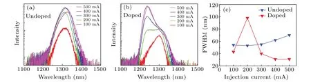
Fig.3.Optical spectra of the(a)undoped and(b)doped CMQD-SLDs(L=3 mm)measured at RT,(c)the corresponding change in the FWHM of(a)and(b),with increasing injection current.

Fig.4. (a)The P-I characteristics of doped CMQD-SLD(L=2 mm)measured at RT under CW and the corresponding change in the FWHM of spectrum of device, with increasing injection current. (b) Optical spectra of doped CMQD-SLD(L=2 mm).
Next, the performance of the doped CMQD-SLD with a shorter cavity of 2 mm is also measured. For the doped CMQD-SLD(L=2 mm),the maximum output power reaches 0.95 mW at 390 mA,as shown in Fig.4(a). The output power of the sample saturates at 390 mA due to the shorter gain length of the sample than that of the above device. Figure 4(b)presents the RT optical spectra of the doped CMQD-SLD(L=2 mm). The spectral variation of the doped CMQD-SLD(L=2 mm)with the injection current follows the same rule as that of the doped CMQD-SLD (L=3 mm) described above.When the injection current is 110 mA,the sample achieves the GS=ES regime,the spectral FWHM is 106 nm,the spectrum dip over 106-nm spans is~0.2 dB, and the output power is 0.11 mW.Figure 4(a)also shows the corresponding change in the FWHM of the spectrum with increasing injection current.The spectral FWHM of the doped CMQD-SLDs all show the same changing law. First, the GS emission is dominant. As the current increases,the peak intensity of the ES is gradually higher than that of the GS,and finally,the ES emission dominates. The broadest spectral FWHM of the sample is wider than that of the doped CMQD-SLD (L=3 mm). The reason is that the length of the straight waveguide of the doped CMQD-SLD (L=3 mm) is longer than that of the sample.The increase in the length of the straight waveguide increases the gain, which is obtained when the light travels back and forth in the waveguide,and increases the proportion of the excited emission,thus reducing the FWHM of the spectrum.
Finally,the facet of the bent region of the doped CMQDSLD (L=2 mm) is covered by antireflection (AR) coating(reflectance below 1%) to reduce the reflection and suppress lasing. The samples are loaded with the p-side up on a thermoelectric cooler (TEC) stage, and the device temperature is maintained at 25°C during the measurements. The output power of the sample is 16.6 mW at 850 mA measured under CW operation at 25°C,as shown in Fig.5(a). Figure 5(b)presents the optical spectra of the sample. When the injection current is 150 mA,the sample achieves the GS=ES regime,with a spectral FWHM of 114 nm,a spectral dip of~0.2 dB in this range and an output power of 0.16 mW.After the spectrum is dominated by the peak of ES, the spectrum width shows a trend of first decreasing and then increasing. When the injected current is greater than 600 mA,the spectrum width increases, which is due to the improved heat dissipation efficiency of the device that enables the injected carriers to be filled to a higher energy level. When the injection current is 850 mA, the spectral FWHM is 114 nm. The active region structure,the quality of the AR coating and the package structure continue to be optimized to achieve higher device performance.

Fig.5. (a)The P-I characteristics of doped CMQD-SLD(L=2 mm)with AR coating measured at RT under CW and the corresponding change in the FWHM of spectrum of device, with increasing injection current. (b)Optical spectra of doped CMQD-SLD(L=2 mm)with AR coating.
4. Conclusion
In conclusion, the InAs/GaAs CMQD-SLDs with and without direct Si doping in QDs are fabricated and characterized, and the results show that the output power of the doped CMQD-SLD is invariably higher than that of the undoped CMQD-SLD under the same injection current. The maximum output power of the doped CMQD-SLD reaches 1.16 mW at 430 mA, while that of the undoped QD-SLD is only 0.06 mW at 290 mA.The maximum spectral FWHM of the doped CMQD-SLD is 98 nm at 200 mA, but it is only 70 nm at 500 mA for the undoped CMQD-SLD.Furthermore,the doped CMQD-SLD has the smallest spectral dip of 0.2 dB at an injection current of 200 mA.We also fabricate CMQDSLDs with a shorter cavity length and obtain a maximum spectral width of 106 nm. In addition, to further optimize the device performance,the facet of the bent region of doped CMQD-SLD is covered by AR coating, and the samples are loaded with the p-side up on a TEC stage. The performance of the doped CMQD-SLD is achieved with a maximum output power of 16.6 mW and a spectral width of 114 nm.
Acknowledgements
Project supported by the National Natural Science Foundation of China (Grant Nos. 62035012, 62074143, and 62004191)and Zhejiang Lab(Grant No.2020LC0AD02).
猜你喜欢
Chinese Physics B(2022年10期)2022-10-26
中华环境(2022年5期)2022-06-01
当代党员(2022年9期)2022-05-20
当代党员(2022年9期)2022-05-20
Chinese Physics B(2022年4期)2022-04-12
中学生数理化·高三版(2021年3期)2021-05-14
校园英语·上旬(2019年2期)2019-04-08
故事会(2015年12期)2015-05-14
浙江人大(2009年3期)2009-04-14
- Chinese Physics B的其它文章
- Characterizing entanglement in non-Hermitian chaotic systems via out-of-time ordered correlators
- Steering quantum nonlocalities of quantum dot system suffering from decoherence
- Probabilistic quantum teleportation of shared quantum secret
- Spin–orbit coupling adjusting topological superfluid of mass-imbalanced Fermi gas
- Improvement of a continuous-variable measurement-device-independent quantum key distribution system via quantum scissors
- An overview of quantum error mitigation formulas