
Native Defect Luminescence of Zinc Oxide Films and Its Potential Application as White Light Sources
2016-07-12 12:43LIUShiCHENYongjianCUIHainingSUNShengnanWANGZihanWANGHaishui
光谱学与光谱分析 2016年5期
LIU Shi,CHEN Yong-jian,CUI Hai-ning*, SUN Sheng-nan,WANG Zi-han,WANG Hai-shui
1.Department of Optical Information Science and Technology, College of Physics,College of Zhaoqing (526061),State Key Laboratory of Superhard Materials, Jilin University,Changchun 130021, China 2.School of Chemistry and Chemical Engineering, South China University of Technology,Guangzhou 510641, China
Native Defect Luminescence of Zinc Oxide Films and Its Potential Application as White Light Sources
LIU Shi1,CHEN Yong-jian1,CUI Hai-ning1*, SUN Sheng-nan1,WANG Zi-han1,WANG Hai-shui2
1.Department of Optical Information Science and Technology, College of Physics,College of Zhaoqing (526061),State Key Laboratory of Superhard Materials, Jilin University,Changchun 130021, China 2.School of Chemistry and Chemical Engineering, South China University of Technology,Guangzhou 510641, China
ZnO light-emitting diodes (LEDs) have an enormous potential in lighting applications.The major issue to be resolved is the generating and control of light emissions.This issue arises from the variation and combination in LED wavelength.We found that defect luminescence of ZnO has a varied wide range of wavelength, which suits to an application of LED for white-light generation.We have shown both experimentally and theoretically that defect emission can be used in ZnO systems.This type of defect has the advantage of not requiring extensive and costly factory systems comparing with traditional doped materials and others.We not only propose potential application of native defect luminescence of Zinc Oxide film for white LEDs-flat light sources, but also have some methods to control defect origins, a certain center position and broad range of the emission band of ZnO film in the initial stage.According to different preparing method and certain experiment conditions, variant white such as whitish and bluish-white etc., primary and important colors- blue bands (455, 458 nm), green bands (517, 548 nm), red bands (613, 569 nm) are obtained respectively.This proved that it is a better road to one white light LED with one kind of material -ZnO.
Defect of ZnO film; Defect luminescence and photoluminescence; White colors LED
Introduction
Researchers have focused on new “low carbon” and “green” material and new kind of white Light-emitting diodes (LEDs) simultaneously, but have generally not realized them becauseof flat material and conceptuallimitations.With the development of flat light sources, it is a new challenge andzigzag story to utilize native defect luminescence of Zinc Oxide (ZnO) film for a potential application as flat white LEDs.Ouraim is to realize white emitting with single material-ZnO film, using its defects.Here, we make schematic diagramsto illustrate the visible and white defect emission of ZnO film.Photoluminescence (PL) spectral studieswere used to analyze the properties of excited states and related native defects.Owing to the built mechanisms with good controllability, we can obtainviolet, blue, green, red emissions and their co-emissions in ZnO film.
In general, LEDs are mainly divided intoinorganic and organic LEDs (OLEDs).In OLEDs, though many groups[1-3]have made great achievements, most of themarestill in the experimental stage.They can not meet industrial requirements for the moment and in the short term.
We have made studies such as optical simulation/optimization of ITO-free top-emitting white OLEDs[4]; white light emission of polythiophenes (PT) at electron beam currents[5]; electroluminescence (EL) characteristics of blend polymer film devices of Al/PT & MEH-PPV/ITO[6]; polymer devices of Al/PT/ITO[7]; efficiency of LEDs based copolymers containing quinoline and pyridine units[8]; effect of annealing of polythiophene derivative for polymer LEDs[9]; a polymeric LED analyzed by a modified SNOM setup[10].In addition, there are size-controlled nanostructures of mixed luminescence polymer films, photoluminescence (PL) study of Langmuir-Blogette films of blend PT, energy transfer in phase-separated luminescent polymer films, and so forth, for OLEDs applications within our research[11-13].Obviously,OLED technology has aroused world-wide attention because it is thought to possess many merits: thin, light in weight, lower costs, no backlight, and easy-to large-scale production; besides, this kind of material can be deposited on flexible plastic substrates.
In inorganic LEDs, many innovative epitaxial processes, designs and materials are being developed and utilized to achieve white light[14].However, there are manydisadvantages of inorganic LEDs: difficult to obtain no (or lower) defect films in the epitaxial growth of AⅢBⅤsemiconductors and others, and to obtain efficient and easy package designs of the white LED structure.These result in the resistance for development of inorganic white LEDs and high price devices[15].
Many innovative epitaxial processes, designs and materials are being developed and utilized to achieve white light in the inorganic LEDs.Development of AⅢBⅤcompound semiconductor technology and their ternary and quaternary alloys incorporated in LED structures are increasing the performance.The majority of recent LEDs are based on AlGaAs/GaAs, AlInGaP/GaAs and InGaN/GaN (gallium nitride) heterojunction devices produced by MOCVD.The wider band gap of nitride semiconductors filled the wavelength gap between the common red-orange-yellow LEDs and the invisible light near UV region[16].Most of the focus on nitride devices (InGaN) is to develop improved or new substrate materials (SiC, etc.) as a substitute for sapphire[17].Another main goal in nitride technology is to use blue LEDs as basic light source in white light devices[18].Also, We have studied and discussed inorganic optoelectronic films and devices, such as (1) ZnCdO, ITO,CdS and different metal oxides thin films for optoelectronic applications[19-27], (2) a nano-sized inorganic/organic complexrectifier with TCNQ/n-Si and/p-Si structure[28], cathodoluminescence spectra of gallium nitride[29].
Scientists are now devising different methods to produce future ZnO LEDs: (1) Bulk ZnO is unavailable in large wafers for the time being; ZnO film has received particular attention as a promising substrate material due to its isomorphic structure and near perfect lattice, matching to GaN[31-32].(2) Primary electroluminescence (EL) from ZnO-based p-n junctions and LEDs[33], and photoluminescence (PL) properties of n-type and p-type ZnO films codoped with N/Al and Ga/N have been reported[34].Clearly, LED based on ZnO thin film, especially for a visible defect emission of ZnO film, may be a relatively new way.
To make conventional white light using LEDs, there are many basic approaches: (1) combining the outputs-two or more LED chips which could be blue and yellow, or more commonly red (R), green (G) and blue (B) by adjusting the mole fraction of doped components in the alloy.It is possible to design light emitting devices covering the visible spectrum.(2) phosphor conversion-a blue LED chip is combined with a phosphor.Some of the blue photons aredown-converted by the phosphor to produce a broad emission centered on yellow; these mixes of yellow and other blue photons look white to the human eyes.(3) using UV LED as a pump chip for a mixture of phosphors that emit across the visible spectrum[30].Clearly, LEDs based on ZnO films, especially defectsand their visible emissions of ZnO, may berelativelynew.
1 Methods
For the electrodeposition deposition of ZnO films, two different procedures were employed.The electrodeposition set-up consists of a three electrode electrochemical cell and a solution containing 25 mmol·L-1ZnCl2, 0.1 mol·L-1KClO4or KCl as supporting electrolyte and oxygen dissolved in dimethylsulfoxide (DMSO) or H2O solution or their mixture.Conductive covered substrates set-up as working electrode were located near the referential cathode.The potentio-static method (constant potential,V=-0.9 V) was used for deposition.During electrodeposition the temperature was maintained at 90 ℃ in a thermostatic bath.
As to the spray pyrolysis deposition of ZnO films, 4×10⁻³mol·L-1of zinc acetate dehydratewas dissolved in ultra pure water.The substrate temperature was (573±2) K.The solution flow rate and gas pressure were kept constant at 50 mL·h-1and 3×10⁵Pa, respectively.The spray nozzle to substrate distance was 10 cm and the spraying time was 30 min.
In the case of the sputtering deposition of ZnO films, a dc/rf magnetron sputtering system was used.The target is a zinc metal disk (50 mm diameter) with a purity of 99.99%, and the vacuum chamber was evacuated down to pressure 1×10⁻³Pa prior to deposition.The sputtering gas (Ar) and reactive gas (O2) were introduced into the chamber separately, and were controlled through two gas mass flow rate controllers.The dc power during the film deposition was 100 W, and the temperature was varied from room temperature (RT) until 300 ℃.
The PL was excited by a He—Cd laser operating at 325 nm and captured by a charge coupled device (CCD) camera through a monochromator.Low temperature PL was performed in a small chamber that could be cooled down to 6 K.
2 Results and Discussions
2.1 Visible Luminescence of ZnO Films
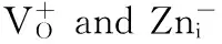
The property of ZnO film defects and their luminescences is very important.Over past decades, ZnOhas attracted the interest of researchers as a potential ultra-violet (UV) optical device material.However, obtaining high quality ZnO materials is the key step of its optoelectronic application.In nature ZnO thin film is only n-type conductivity due to a large number of defects, such as oxygen vacancy (VO) and interstitial zinc (Zni), which lead to difficulty in achieving p-type ZnO thin film.The deficiencies involving radiative and nonradiative defects and impurities, mainly degrade the near band edge (NBE) luminescence.In general, the visible emission is attributed to the native defects in ZnO.Based on these points, more work is focused upon excitons and NBE, as well as deep level emission (DLE),which play an important role in evaluating crystal quality and material structures.Recent papershave reported the introduction of particle irradiation such aselectrons[35]and ions[36]injections to ZnO increases the concentration of defects, and contributes to PL improvement.It is interesting and significant to clarify various behaviors of the crystal, defects, microstructure and their relative luminescence characteristics.

Fig.1 Photoluminescence (PL) Spectra of the ZnO films
One of the major difficulties in producing ZnOLEDsis the lack of ideal crystal materials or crystal films.This is due to structural defects from the growth process.The objective of any film growth is to minimize the defect densities and lower the intrinsic perturbations to the lattice.Herein, we propose that it is by employing the native defect emission to obtain visible emission in green, yellow and orange regions, that extend visible luminescence range in ZnO film.These films are suitable to serve as future light sources-white LEDs, especially flat light source with large areas and panel displays.Defect studies such as relationships among defect processing, chemistry and physics, have been considered in scientific and technological areas, but novel applications of defect have not received much attention.It is quite vital to investigate the optical properties-different visible spectrum range for variant native defect of ZnO films, in order to design workable white LED.A detailed understanding of the emission mechanism in ZnO materials is very important not only for physics, but also for the fabrication of well-designed and easily-processed LEDs.
It is reported that both PL and electroluminescence (EL) originate from the radiation recombination of exciton states and PL study results are in consistent with EL’s[1, 37].The PL spectra of ZnO films werestudied from lower temperature 6 to 300 K.According to Table 1, Sample S1, S2, S3 and S4 are of white emissions [Fig.1(a), (b), (d)] orquasi-white [Fig.1(c)] at room temperatureasthe descriptionin color theory.White, as a neutral color in color theory, is a balanced combination of all colors in the visible light spectrum, or a pair of complementary colors, or three or more colors, such as additive primary colors in Fig.7.Also, they could be combination of blue and “cadmium yellow (CY)”; green and “deep pink (DP)”; red and “electric cyan(EC)” from the additive color mixing system (Fig.7).

Table 1 Sample information
A color can be defined as a class of spectra that give rise to the same color sensation, even though suci classes would vary widely among different species.Humans can recognize colors approximately from 380 to 750 nm.The “color” definedby classes of spectra are shown in Fig.8.Generally, narrow triband illuminants consisting of three “narrowband” emissions are caused by ternary compositions of phosphors in the R-G-B regions of the visible spectrum.By tuning the phosphor ratios with desired correlated color temperatures, the expected white light source can be achieved.
Obviously, Fig.1(b) indicates the existence of three main components whose centers of the wide emission bands locate at 413, 560 and 692 nm; Fig.1(a) reveals the existence of three components 401, 562 and 675 nm in the emission bands; Fig.1(d) shows the existence of 400, 528 and 714 nm wide emission bands.Further simulation study with three Gaussian peaks fitting for integrated intensity in the range of 350~770 nm for the curve of Fig.1(c) were accomplished, and it revealed 417, 510 and 712 nm emissions (dash line).These three wide bands are a mixture of blue-violet, green and red.Differentkinds of white light mentioned above are obtained respectively.
Comparing with conventional hetero junction white light LEDsin Fig.2(a), we can also obtainsimilar PL spectrum in Fig.2(b) (sample S5 in Table 1).In both Fig.2(a) and (b), a prominent and a broader band can be observed in the visible PL spectrum.In Fig.2(b) the prominent one is a blue-violet emission whose centre isaround 410 nm, and the broader one is visible emissioncovering from 450 to 780 nm wavelength range.
According to previous reports, obtaining such different white emissions is infrequent.All the adopted strategies, which mean to produce white light by color blending, are complex in sequent device fabrication process compared with using the native defect luminescence of ZnO film.Since three materials emitting red, green, and blue, can be combined to produce white, different research groups have adopted the blending of colors in LEDs to produce white light in diverse strategies.They are: (1) dyes or phosphors canbe mixed in the emissive layer of the LED to convert, under specific condition, many kinds of colors to white; (2) individual R-G-B components (side-by-side or stacked) will allow users to set their own color balance for LEDs; (3) R-G-B pixels can be arranged side-by-side or stacked, similar to the techniques used to make flat-panel displays for obtaining white LEDs; (4) for transparent devices, colors can be combined by stacking pixels one on top of another.

Fig.2(a) A white spectrum of conventional heterojunction LEDs
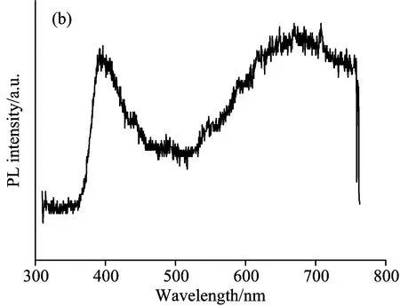
Fig.2(b) Similar PL spectrum of ZnO (sample S5) compared with Fig.4(a).It was deposited by Spry method on a modified ITO substrate
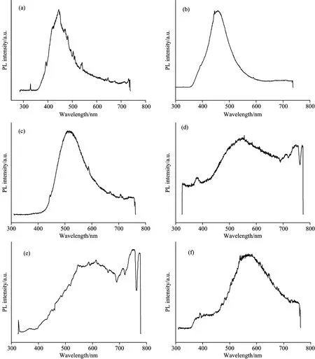
Fig.3 Typical and primary colors- blue, green and red PL of ZnO films
Here, we can realize a variant luminous film material by adjusting and controlling conditions of ZnO preparation.Fig.3 presents the typical and primary colors- blue, green and red PL of ZnO films.In sample S6—smaple S11 of table 1,broad blue bands (455, 443 nm), green bands (517, 548 nm), red bands (613 nm) and yellow (569 nm) show prominent emission respectively,employing certain conditions and preparation methods by the order.The luminescence of primary colorsis very crucial for white sources andthe base of obtaining and adjusting required emission band.
2.2 Exciton and Defect Levels of ZnO Film
PL spectra come from optical transitions which include excitonsand defect levels, that is, excitonic part and defect part form all PL regions.
There are free exciton (FE), bound exciton (BE) and localized exciton (LE) emissions.Traditionally, NBE and exciton are the elementary parts of PL investigations, and used to study optical transitions and quality of ZnO materials.
In fact, the NBE band is relatively wide emissions, which are related to the free exciton (FE) emission.It consists of bound exciton (BE) or BE-based complex emissions.The BE emission comes from the impurities (donor or acceptor)[38].The 387 nm peak belongs to signal crystal ZnO and is the intrinsic optical property of ZnO crystallites[39].It corresponds to some kinds of varieties of 357 nm (3.48 eV) FE plus three longitudinal optical (LO) phonon replica by the calculation of 72 meV phonon energy[40].Also, it is attributed to BE emissions in ZnO films.The emission at 370 nm (3.36 eV) is well known as BE that is usually dominant in low temperature PL of crystal ZnO materials.
For the polycrystalline ZnO film condition, the “recombination of electrons and electron holes” leads to a formation of excitons (or excited states) consisting of bound electrons and holes.Due to exciton binding energy and the lattice relaxation, the luminescence energy of ZnO is usually lower than the HOMO-LUMO band gap, which is around 3.5 eV for a crystalline of ZnO.When the exciton energy is transferred from the high level to the deep level, the defect level produces radiation in the decay process tothe ground state.
The emissions of ZnO films are come from several excitonic recombinations where BE to defect levels or valence band, which are assigned to the transitions involved in defects.The PL spectra were used to analyze the properties of excited states and related native defects since it is a very sensitive tool for characterizing radiative deficiencies.Further spectral studies, including the effect of annealing and excitation, were implemented in the work.
Though our work is focused on defect emissions, we have to mention exciton and the near band edge (NBE), because they have a certain relationship with some visible luminous band in the short wavelength region.At the same time, they can also assess defects of ZnO films.
A further spectrum analysis on the curve of Fig.2(b) should be carried out, because short-wavelength prominent band is complex.The Gaussian fitting is shown in Fig.4, which indicates that three sub-bands in the violet 387 nm (3.21 eV) and green-violet 403 nm (3.08 eV) andgreen 442 nm (2.81 eV) regions form 410 nm emission.Analysis results tell us that 410 nm band is not an variant of an usual (intrinsic/ordinary) NBE band (from 3.33 to 3.10 eV) of ZnO films in the near UV region, and it is a mixture of 387 nm NBE, 403 nm LE complex and 442 nm deep level emission (DLE) at room temperature.The emission near 403 nm (3.08 eV) has been ascribed to recombination of localized exciton (LE) complex[41], and it could be from band-to-band recombination in the quantum confinement effect of nano-crystalline or nano-grain.In the present work, however, the dominant emission is the broad band at 403 nm (3.08 eV) and 442 nm (2.81 eV), the 387 nm (3.21 eV) NBE becomes weak.In Fig.4, the 387 nm NBE shows an average room temperature PL linewidth of about 130 meV.Compared with the values obtained from ZnO films prepared by other methods like plasma-enhanced chemical vapor deposition and sputtering in which the NBE of the film was much broader, it indicates a poorer crystalline quality[42-43]or nanocrystal materials.In general,a strong NBE demonstrates good optical quality ZnO.The PL of ZnO is dominated by BE lines, and a broader visible band springs from defect states which belong to DLE as Fig.2(b).Here the room temperature PL for the sample S2 [Fig.1(b)] is composed of the 387 nm band and visible broader band in a long wavelength region.A decreasing tendency of 387 nm NBE/visible broader (450~780 nm) DLE, in contrast with that (two main prominent bands consist of narrow NBE and visible broader DLE) of other crystal ZnO films, means that there exists more defect concentrationin this ZnO film.

Fig.4 A further spectrum analysis on the complex curve -410 nm prominent band of Fig.2(b)
In order to investigate the real phenomenon and trend of defect events, further PL spectra of ZnO film samples S1, S2 and S3 were measured at lower different temperatures in all the visible range, as shown in Fig.5.Emission bands of samples S1, S2 and S3 increase remarkably when the temperature of measurement decreases from 250 K to 6 K.Since a prominentlybroader DLEband centered near 405 nm is observed in PL spectra at lower temperature, it demonstrates theexistence of a good optical quality ZnO for these samples.In Fig.5(a) and (b), proportional intensityincrease of other visible wide bands with the decrease of temperature at much longer wavelength center position exhibits that samples have some stable defects and these PL come from defect emissions.

Fig.5 PL spectra of ZnO film samples S1, S2 and S3 [Fig.1(a), (b), (c)] measured at lower temperatures (from 250 to 6 K) in all the visible range

ZnO⟺VO+VZn+Zni+Oi
(5)

(6)

(7)

(8)

(9)
(10)
(11)

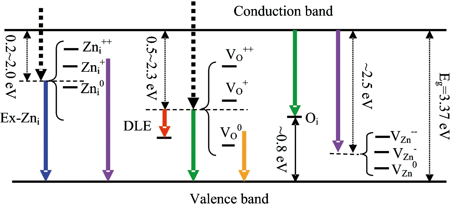
Fig.6 A possible energy leveldiagram of native defects inside ZnO band gap with corresponding schematic band of relevant visible emissions
2.3 Defect/Structure Characterizations and Violet/Blue Emissions
Most of the contributors believe that common native defects in stable ZnO are VO, VZn, Zniand Oi.A possible energy level diagram inside ZnO band gap, which obtained by summing up all achievements such as the theoretical computation with First principle calculations[46-48]and experiments[45,49], are shown in Fig.6.Theoretical calculations predicted and experimental results determined Znilevel is in a range of 0.2~2.0 eV below the conduction band bottom.The energy variance from conduction band bottomto the VZnlevel is about 2.50~3.07 eV.
Znilevel positions are in agreement with the 455 nm (2.73 eV) and 443 nm (2.80 eV) blue or violet-blue emissions of sample S6 and S7 from Fig.3(a) and (b).Since the high deposition rate of sputtering processbrings high concentration of Zniwith different charges-neutral, single and double valence, theyderive from transitions correlating Znidefect states.In addition, the previous 443 and 455 nm emissions may also comefrom transitions between “extended Zni” (Ex-Zni) states level andvalence band.
Because ZnO has a relatively open lattice structure with octahedral and tetrahedral sites for Zniatoms, the octahedral sites are stable positions for Zniand tetrahedral sites could be mobile and unstable positions for Zniin ZnO[50].However, the existence of Zniin grain boundaries is possible to some extent.There could also be several derivative levels with lower energies involved in localization or coupling with other defects, and all above lead to variant emissions.
The 443 nm (2.80 eV) and 455 nm (2.73 eV) emissions were from transitions between Znior “extended Zni” (Ex-Zni) states level and VB, respectively.Blue emissions attributed to the transition from “Ex-Zni”states are slightly around the ordinary Znistate.These extended states can form during the various preparation processes or post-treatments, according to the defect ionization reaction Equation (8) and (9), and can result in defect localization coupled with a disordered lattice.Here, the “Ex- Zni” states could be ionized Zni, complex defect or localized Znistates.
As we know, transitions of defects include radiative and non-radiative emissions that come from difference of levels.According tothe foregoing statement, The electrons in the conduction band relax (non-radiative) to Znistate.After that, they relax to “Ex- Zni” states, and then transit to valence band with blue emissions.Similarly, for the violet emissions [411 nm of Fig.1(b), etc.], if the electrons are excited up to a sub-band of the conduction band, they can relax to Znistate through a nonradiative transition, and finally transit to valence band.
Corresponding transmissions with relvent blue-violet and blue emissonsare shown in Fig.6.The electrons in the conduction band relax (non-radiative) to Znistate, and then in a sequel to (or directly relax to) “Ex-Zni” states.Finally, they transit to valence band and emit blue lightsuch as 455 nm of Fig.3(a).
水库流域涉及太谷、榆社、祁县三县地域,农田种植施用化肥、农药,养殖牲畜排放粪便、堆放存储垃圾、污染物,易对水体造成污染。

Fig.7 Whiteas a neutral color in a balanced combination of a pair of complementary colors, or three or more colorssuch as additive primary color mixing system
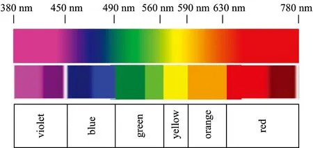
Fig.8 The defined color followed by classes of spectra in a visible spectrum range
2.4 Defect/Structure Characterizations and Green/RedEmissions
In Fig.3 (c) and (d), 517 and 548 nm green emissionsmay be from the transitionsbetween the conduction band anddeep level like Oiof Fig.6.The DLE involves deep trapped charged carriers in ZnO[51].For possible green emissions, there is another process.The electrons excited up to a sub-band of the conduction band can relax to VOstate through a non-radiative transition, and then transit to VB.Both explanations have a relationship with oxygen.

Fig.9 PL spectra of ZnO film samples S10 measured at lower temperatures (from 250 to 7 K) in all the visible range
For red emission, the band at around 639 nm had been observed in the PL spectra of ZnO.It indicates the existence of macrocrystal line ZnO and confirms the high dispersion (discrete column) of ZnO[52].Further lower temperature PL experiments of sample S10 were carried out, and their spectra are shown in Fig.9.A shift to long wavelength direction, peak increase and a narrow DLE peak at around 613 nm (2.03 eV) appears when the temperature of measurement decreases from 250 to 6 K.This sort of behavior indicates defects involved emission.

3 Further Discussion and Conclusions
Our explanationshave been further proved in studies on protonimplanting, positron annihilation, electron/ion injections inZnO films and their electrical property investigations.Our PL explanationshave been further proved in studies on protonimplanting, positron annihilation, electron/ion injections inZnO films and their electrical property investigations.Researches on artificial defects where protons were implanted into single crystal of ZnO, were studied by Auret, etc.[56].Orange-red DLE bands became apparent in the PL spectra of protons implanted into ZnO, and they were still present even after most of the protons were removed by annealing at 700 ℃.Clearly it show us that the PL comes from the defects created.In recent papers, it is reported by authors that the introduction of particle, such as electron[57]and ion injection[58]to ZnO increases concentration of defects, resulting in PL improvement.VZnhas also been detected by positron annihilation spectroscopy to be one of the main defects in ZnO films.Likewise, Vlasenko and Watkins[59]also found that electron irradiation produced VOand other defectsin ZnO, leading to a reduction in green luminousness and an increase in PL bands near 600 and 700 nm.
To analyze and explain the defects we measure electrical resistivity of ZnO films too.As we know, ZnO films show n-type conduction as determined bysign of Hall-coefficient.The reason for this is formationof shallow donors associated with VOand Zniatoms.Hence, free carriers in ZnO originating from VOare possible cause of lower electrical resistivity.Oxygen annealing of as-deposited ZnO films increases electrical resistivity in our experiments.This increase in resistivity by oxygenation is due to compensation of free carriers through reduction in VO[60].In addition, the sample deposited at 200 ℃ shows poor conductivity giving evidence that VOis a deep donor.Decrease in conductivity of annealed ZnO films show that VOis primary defect.
These work squestioned the assumption -green luminousness is onlyrelated to VO.Our result suggests that there are intrinsic Zni, VO, VZnand other defects in the pure ZnO film.Regarding defect origin process related itsluminousness, they could be: (1) in preparation of films, two factors including high temperature and pressure plasma conditions (plasma sources, or a great energy beam) and rapid formation rate of the ZnO films can lead to thermodynamic growth of films, which will deviate greatly from the equilibrium states.Thus, the non-equilibrium processes can induce a high concentration of special defects which is favorable to the visible luminescence.(2) the lattice mismatch and difference in thermal diffusion/expansion coefficients between ZnO and modified surface of substrates could possibly be the cause of defect forming during growth of films.These affect ZnO films and its properties such as excitonic binding energy, surface microstructures and crystalline structures.
All results and discussions have shown that the deposited ZnO films have different defect styles and microstructures.These defectstates exhibit three primary colors andvariant white such as whitish and bluish-white.They can be adapted by preparing methods, conditions and post-treatments like annealing temperature; when changing the relevant selection of them, we can control the visible emissions of ZnO films effectively.This study may deepen the understanding of defect- related visible emissions in ZnO, and extend the white LEDs with easy fabrication in one kind of ZnO film material.
[1] Akcelrud L.Prog.Polym.Sci.2003,28:875.
[2] Shufen C, Lingling D, Jun X, et al.Adv.Mater., 2010, 22: 5227.
[3] Gather M, K?hnen A, Meerholz K.Adv.Mater.,2011,23:233.
[4] Ma J, Piao X, Liu J, et al.Organic Electronics,2011,12:923.
[5] Panin G N, Kang T W, Lee H.Physica E,2004,21:1074.
[6] Ahn T K, Han S H, Lee H.Mol.Cryst.Liq.Cryst.,2002,377:391.
[7] Ahn T K, Choi B S, Ahn S H, et al.Synthetic Metals,2011,117:219.
[8] Kim D Y, Lee S K, Kim J L, et al.Synthetic Metals,2001,121:1707.
[9] Ahn T K, Lee H, Han S H.Appl.Phys.Lett.,2002,80:392.
[10] Micheletto R, Yoshimatsu N, Yokokawa M, et al.Optics Communications,2001,196:47.
[11] Cui H N, Teixeira V, Zhang J, et al.Thin Solid Films,2006,515:301.
[12] Cui H N, Lee H.Mol.Cryst.Liq.Cryst.,2000,349:475.
[13] Cui H N, Lee H.Synthetic.Metals,2001,117(1-3):255.
[14] Schubert E Fred.Light-Emitting Diodes.Cambridge University,2006.422.
[15] Steranka F.Opto & Laser Europe,2003.
[16] Cook M.Review,2006,29(5):22.
[17] Stath N, et.al.Materials Science and Engineering,2001,B80(1-3):224.
[18] Akasaki I.J.of Cryst.Growth,2002,237-239(4):905.
[19] María B, Tortosa M, Mollar M, et al.Optical Materials,2010,32:1423.
[20] Cui H N, Teixeira V, Meng L J, et al.Thin Solid Films,2008,516:1484.
[21] Cui H N.Optical Multilayered Coatings for Application of Smart Windows, Subtitle-Preparation and Characterization.VDM Publishing House Ltd.Germany,2009.
[22] Teixeira V, Cui H N, Meng L J, et al.Thin Solid Films,2002,420-421:70.
[23] Cui H N, Xi S Q.Thin Solid Films,1996,288:325.
[24] Cui H N, Jia S, Meng L J, et al.Mikrochimica Acta,2004,145:19.
[25] María B, Tortosa M, Mollar M, et al.Optical Materials,2010,32:1423.
[26] Teixeira V, Cui H N, Meng L J, et al.Thin Solid Films,2002,420-421:70.
[27] Cembrero J, Elmanouni A, Hartiti B, et al.Thin Solid Films,2004,451-452:198.
[28] Lee H S, Lee N, Lee H W, et al.Mol.Cryst.Liq.Cryst., 2002,377:25.
[29] Manjón F J, Hernández-Fenollosa M A, Marí B, et al.The European Physical Journal B,2004,40:453.
[30] Whitaker T.Innovations Push White LEDs Towards New Applications.Compound Semiconductor,2003.
[31] Detchprohm T, Hiramatsu K, Amano H, et al.Appl.Phys.Lett.,1992,61:2688.
[32] Xiao R F, Sun X W, Liao H B, et al.J.Appl.Phys.,1996,80:4226.
[33] Ryu Y R, Lee T S, Lubguban J A, et al.Appl.Phys.Lett.,2006,88:241108.
[34] Yan Y F, Li J B, Wei S H, et al.Phys.Rev.Lett.,2007,98:135506.
[35] Hernández M A, Damonte L C, Marí B.Superlattices and Microstructures,2005,38:336.
[36] Damonte L C, Hernández M A, Marí B.Journal of Alloys and Compounds, 2007,434-435:813.
[37] Bradley D C.Chem.Brit.,1991,27:719.
[38] Ryu Y R, Lee T S, White H W.Appl.Phys.Lett.,2003,83:87.
[39] Wang X, Summers C J, Wang Z L.Adv.Mater.,2004,16:1215.
[40] Dai J, Su H, Wang L, et al.J.Cryst.Growth,2006,290:426.
[41] He H P, Ye Z Z, Zhuge F, et al.Solid State Commun.,2006,138:542.
[42] Liu X, Wu X, Cao H, et al.J.Appl.Phys.,2004,95:3141.
[43] Choi C H, Kim S H.J.Cryst.Growth,2005,283:170.
[44] Kang H S, Kang J S, Kim J W, et al.J.Appl.Phys.,2003,95:1246.
[45] Look D C, Falow G C, Reunchan P, et al.Phys.Rev.Lett.,2005,95:225502.
[46] Janotti A, Van de Walle C G.Appl.Phys.Lett.,2005,87:122102.
[47] Bylander F G.J.Appl.Phys.,1978,49:1188.
[48] Lin B, Fu Z, Jia Y.Appl.Phys.Lett.,2001,79943.
[49] Vlasenko L S, Watkins G D.Phys.Rev.B,2005,71:125210.
[50] Look D C, Farlow G C, Reunchan P, et al.Phys.Rev.Lett.,2005,95:225502.
[51] van Dijken A, Meulenkamp E A, Vanmaekelbergh D, et al.J.Lumin.,2000,90:123.
[52] Chen J, Feng Z, Ying P, et al.J.Phys.Chem.B, 2004, 108: 12669.
[53] Vanheusden K, Warren W L, Seager C H, et al.J.Appl.Phys.,1996,79:7983.
[54] Liu M, Kitai A H, Mascher P.J.Lumin.,1992,54:35.
[55] Özgür Ü, Alivov Y, Liu C, et al.J.Appl.Phys.,2005,98:041301.
[56] Auret F D, Goodman S A, Hayes M, et al.Appl.Phys.Lett.,2001,79:3074.
[57] Hernández M A, Damonte L C, Marí B.Superlattices and Microstructures,2005,38:336.
[58] Damonte L C, Hernández M A, Marí B.Journal of Alloys and Compounds, 2007, 434-435: 813.
[59] Vlasenko L S, Watkins G D.Phys.Rev.B,2005,71:125210.
[60] Choopan S, Vispute R D, Noch W, et al.Appl.Phys.Lett.,1995,75:3947.
O462.3
A
氧化锌薄膜的缺陷发光和它作为白光光源的潜在应用
刘 石1, 陈永健1,崔海宁1*,孙胜男1,王子涵1,王海水2
1.吉林大学物理学院光信息科学与技术系(肇庆学院,626061)超硬材料重点实验室,吉林 长春 130021 2.华南理工大学化学与化学工程学院,广东 广州 510641
ZnO发光二极管(LEDs)在照明应用方面有着巨大的潜力。需要解决的主要问题是光的产生和对辐射的控制,这个问题来自LED波长的变化和组合。发现缺陷发光的ZnO有着各种波长范围,适合LED在白光产生方面的应用。同时展示了在实验和理论上可以用于ZnO系统的缺陷辐射。这种类型的缺陷相较于传统的掺杂材料和其他材料,其优点在于不需要广泛和昂贵的生产系统。不仅提出了ZnO薄膜在白色平面LED光源本征缺陷发光的潜在应用,同时也利用一些方法一个特定的中心位置和ZnO薄膜在初期发射谱带的宽分布来控制缺陷的产生。根据不同的制备方法和特定的实验条件,不同的白色,如稍白色和青白色等原本的和重要的颜色-蓝光波段(455, 458 nm),绿光波段(517, 548 nm),红光波段(613, 569 nm)分别被获得。从而说明了这是一种制作白光LED更好的办法-利用ZnO材料。在对ZnO薄膜电学性质的调查研究中,通过薄膜表面的额电子插入和正离子的湮灭已经证明了的观点,随着质子的植入、正离子的湮没、电子的插入和ZnO表面的电学性质的研究,表述结果被进一步的证实。研究人员对单晶ZnO的已经有了一定的研究,PL质子植入ZnO以后呈现橘红色,并且在700 ℃退火后仍然存在,清楚的可以看出PL缺陷的存在。在植入粒子方面最近的文章也有报道,例如在ZnO缺陷表层中注入离子和电子来改变PL性能。VZn也发现了氧化锌薄膜的主要缺陷之一是正电子湮没,同样的,Vlasenko和Watkins也发现了氧化锌表面由于电子辐射产生的缺陷。导致绿色透光率的减少,增加PL致600~700 nm。之后分析和解释ZnO薄膜电阻率的缺陷。由霍尔系数的迹象表明ZnO表现为N型传导,这样做的原因是因为把VO和Zn原子联系在一起,使Zn具有较低的电阻率。试验中氧气退货可以增加ZnO的电阻率,其电阻率的增加是由于VO的减少。另外,在200 ℃条件下准备的样品导电率很低,说明了VO的作用很大。退火氧化锌薄膜电导率下降表明, 看到了主要的缺陷。
氧化锌薄膜的缺陷; 缺陷发光与光致发光; 白光LED
2015-09-01,
2015-12-30)
Foundation item:Jointly Funded Project (61179055) of Chinese Civil Aviation Authority and National Natural Science Foundation of China, Grant (2012B040303007) of Science and Technology Planning Project of Guangdong Province and Talent Grant (2013-ZQXY-05) of Educational Commission of Guangdong Province, China
10.3964/j.issn.1000-0593(2016)05-1604-11
Received:2015-09-01; accepted:2015-12-30
Biography:LIU Shi, (1987—), a PhD student studying in Department of Optical Information Science and Technology, College of Physics, Jilin University *Corresponding author e-mail: cuihaining2009@126.com
*通讯联系人
猜你喜欢
——碳正离子的产生及稳定性比较
高中数理化(2022年20期)2022-11-17
中华民居(2021年4期)2021-11-18
云南化工(2020年11期)2021-01-14
天津化工(2020年5期)2020-10-15
广州化工(2020年8期)2020-05-13
照明工程学报(2016年3期)2016-06-01
现代工业经济和信息化(2016年1期)2016-05-17
连环画报(2016年4期)2016-05-05
通信电源技术(2016年3期)2016-03-26
中国房地产业(2016年9期)2016-03-01

- 光谱学与光谱分析的其它文章
- Pb(Ⅱ)印迹磁性复合吸附剂在水溶液中吸附行为的FAAS法分析
- Study on the Multi-Spectral True Temperature Pyrometer for Explosion Transient of Thermo-Baric Explosives
- 蛋白饲料原料粗蛋白含量近红外光谱模型转移研究
- 小波变换和连续投影算法在火龙果总酸无损检测中的应用
- 增强的UV-B辐射对高粱幼苗光合和抗氧化系统的影响
- Spectrum Quantitative Analysis Based on Bootstrap-SVM Model with Small Sample Set