
Extrinsic equivalent circuit modeling of InP HEMTs based on full-wave electromagnetic simulation
2022-04-12 03:44ShiYuFeng冯识谕YongBoSu苏永波PengDing丁芃JingTaoZhou周静涛SongAngPeng彭松昂WuChangDing丁武昌andZhiJin金智
Chinese Physics B 2022年4期
关键词:武昌
Shi-Yu Feng(冯识谕) Yong-Bo Su(苏永波) Peng Ding(丁芃) Jing-Tao Zhou(周静涛)Song-Ang Peng(彭松昂) Wu-Chang Ding(丁武昌) and Zhi Jin(金智)
1University of Chinese Academic of Sciences,Beijing 100029,China
2High-Frequency High-Voltage Device and Integrated Circuits Center,Institute of Microelectronics,Chinese Academy of Sciences,Beijing 100029,China
Keywords: extrinsic equivalent circuit modeling,InP HEMT,HFSS and ADS co-simulation,S-parameters
1. Introduction
Indium-phosphide-based high-electron-mobility transistors(InP HEMTs)with outstanding high-frequency characteristics have been developed and widely investigated in the last decades. Now,the InP HEMT possesses cut-off frequency up to hundreds of gigahertz and maximum oscillation frequency over 1 THz.[1-3]And the high-frequency InP HEMT has been designed and manufactured into sub-millimeter monolithic integrated circuits(MMIC).[4-6]However, as the operating frequency of the device continues to increase, the device exhibits a distributed behavior, and the parasitic resistance, capacitance,and inductance of the metal plating layer interconnected with the device make the performance of the device degrade significantly.[7]Moreover,the conventional device models can no longer characterize the basic physical principles of device performance degradation. Hence, high-fidelity smallsignal device models,in which intrinsic and extrinsic behavior concurrently are considered, are necessary for effectively designing the high-frequency band integrated circuits.
The small-signal model of InP HEMTs can be divided into nonlinear intrinsic elements and linear extrinsic parasitic couplings.[8]The extrinsic elements are independent of the bias voltage,but they basically depend on the physical geometry of the device,including interconnections,electrode structures, and pads. Therefore, the extrinsic parasitic parameters are first proposed and subtracted from the experimental data when modeling. Subsequently, the intrinsic elements related to the bias are determined according to the applied bias voltage. This shows that any calculation errors of external parasitic parameters will lead to errors in the intrinsic parameters of the device and thus affecting the correct understanding of the inherent performance of the device. Hence, the accurate modeling of extrinsic parasitic components is essential.
In the past, the small-signal equivalent circuit model of InP HEMTs is established on the basis of device measurement.[9-11]When using the measuredS-parameters to extract the equivalent circuit,there appears a problem that the unknown parameters in the circuit model are more than the number of equations provided by the experimental data.[12]In order to avoid this problem, a numerical optimization algorithm is used to extract the extrinsic parasitic parameters.However, the extraction results of numerical optimization methods are easily affected by the initial values of the parameters. More importantly, the model established by the device measurement matches the device model, which is provided only by the device manufacturer,and cannot be applied to any other device.Hence,there is needed a modeling technique that is not affected by the device model while ensuring the modeling accuracy.
The primary purpose of this paper is to explore the InP HEMT’s extrinsic parasitic equivalent circuit model through electromagnetic(EM)simulation. On the basis of the conventional HEMT’s model, by HFSS and ADS co-simulation, the frequency response of InP HEMT device’s parasitic coupling in the low-microwave range and the mmW frequency range are predicted. Based on the parasitic coupling effect,the extrinsic parasitic parameters of InP HEMT are extracted and the parasitic equivalent circuit model is established. By comparing the co-simulation results and complete experimental data,the feasibility of parameter extraction and the accuracy of the parasitic equivalent circuit model are verified. Finally,the utility of HFSS and ADS co-simulation results of InP HEMTs model is demonstrated through an example. In the frequency range below 40 GHz which is limited by measurement condition in our laboratory, the proposed method proves highly accurate for a resistive passive device with highly distributed embedding surroundings.
2. InP HEMT’s extrinsic parasitic equivalent circuit model
A cross-sectional view of the InP HEMT is shown in Fig. 1. The epitaxial layer structure is grown by molecular beam epitaxy (MBE) on a 3-inch (1 inch=2.54 cm) semiinsulating(100)InP substrate.[13]The epitaxial layers consists of,from the bottom to the top,a 500-nm InAlAs buffer,a 15-nm In0.53Ga0.47As channel layer,a 3-nm InAlAs spacer layer,an 8-nm InAlAs Schottky barrier layer, a 4-nm InP etching stopper layer, and a 20-nm Si-doped composite InGaAs cap layer.An Si-doped plane is inserted between the Schottky barrier layer and the spacer layer to supply the electrons for current conduction. All InAlAs layers are lattice-matched with the InP substrate.
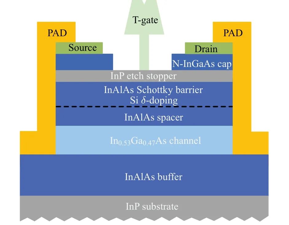
Fig.1. Cross-sectional view of InP-based HEMT.
The extrinsic parasitic equivalent circuit of InP HEMT is independent of the external bias. Therefore, when analyzing the parasitic equivalent circuit,the device can be considered to be in a non-conducting state, which can be seen as a simplified geometric structure composed of metal and substrate as shown in Fig. 2(b).[14]To better demonstrate the distributed and mmW radio-frequency (RF) behavior of the device, the metal sizesd1,d2, andd3are set to be 40 µm, 200 µm, and 60µm respectively. The representative geometric structure is simulated in HFSS to obtain the simulation data, which are then imported into ADS to determine the extrinsic equivalent circuit components of InP HEMT,and finally an external parasitic circuit model is established.
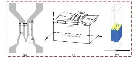
Fig.2. (a)Simplified three-dimensional schematic diagram of InP HEMT with two fingers whose geometry dimensions are w1 =6µm, w2 =4µm,s1=s2=4µm,d1=40µm,d2=200µm,d3=60µm;(b)InP HEMT structure diagram;and(c)simulation structure diagram of InP HEMT in HFSS.
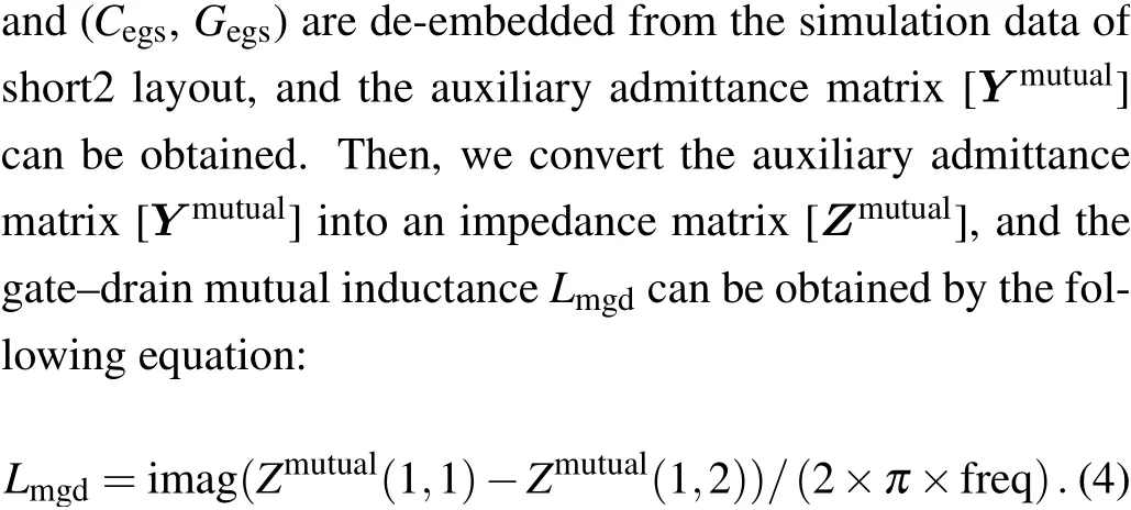
The extrinsic parasitic model of the improved InP HEMTs, shown in Fig. 3, involves 19 circuit elements. At high frequencies, the capacitive elements in the conventional HEMT equivalent circuit model are likely to shunt out the inherent transconductance,which provides the gain mechanism of the device.[15]Therefore,a conductive element corresponding to the capacitive element is introduced into the external parasitic circuit. Capacitive elementsCegs,Cegd, andCedsare inter-electrode capacitances,representing the fringing electric field between the gate, drain, and source. The corresponding conductivity componentsGegs,Gegd, andGedsare the interelectrode conductances, which are used to characterize the conduction currents between the gate,drain,and source due to damage to the substrate. The electrical couplings between the gate, drain, and source contact pads are characterized by capacitive elementsCpgs,Cpgd,andCpds.The corresponding conductivity componentsGpgs,Gpgd, andGpdsare the inter-pad conductivities, which represent the electrolyte leakage losses caused by the conductivity of the semiconductor substrate.The resistive elementsReg,Red, andReshave physical meanings for the power consumption of the gate,drain,and source structure and the surrounding environment.The inductance elementsLeg,Led,andLesare electrode inductances,representing the energy stored respectively in the magnetic field around the current-carrying gate,drain,and source.Most importantly,Lmgdis introduced to simulate the magnetic flux between the gate and the drain.
C
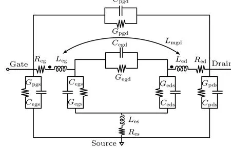
Fig.3. Improved equivalent-circuit model for InP HEMT describing extrinsic parasitic couplings.
3. Extract extrinsic parasitic circuit components using representative test structures
Conventional InP HEMT extrinsic parameters are determined by using a cold HEMT atVds=0,Vgs=0,and pinchoff voltage.[16]Although cold HEMT conditions can be easily achieved when a probe test bench is used for testing, the de-embedding problems and some pad parasitic effects can be brought in, making the process of determining extrinsic parasitic parameters complicated and inaccurate.[17]At the same time, a large number of circuit elements that need to be concurrently determined make the single-step parameterextraction procedure rather sensitive and unreliable. Here, a multi-step method is used to strategically divide the external circuit model into multiple sub-circuits, which can be easily adapted to experimental or simulation data to determine the frequency-dependent parasitic components of the InP HEMTs.The six proposed layouts of the algorithm are implemented in HFSS,and the corresponding lumped-element equivalent circuits for each of the test layouts are given in the ADS. The six proposed layouts and corresponding equivalent circuits are given in Figs.4 and 5,respectively.

Fig. 4. Schematic diagram of the representative test structure of the proposed InP HEMTs: (a)pad, (b)thru1, (c)thru2, (d)short1, (e)short2, and(f)open test.
In the first step,the parasitic admittance matrix[Ypad]of the pad is obtained by the HFSS simulation of the pad structure in Fig.4(a). The parasitic capacitance and conductance of the corresponding padtopad in Fig.5(a)are extracted from the the following equations:

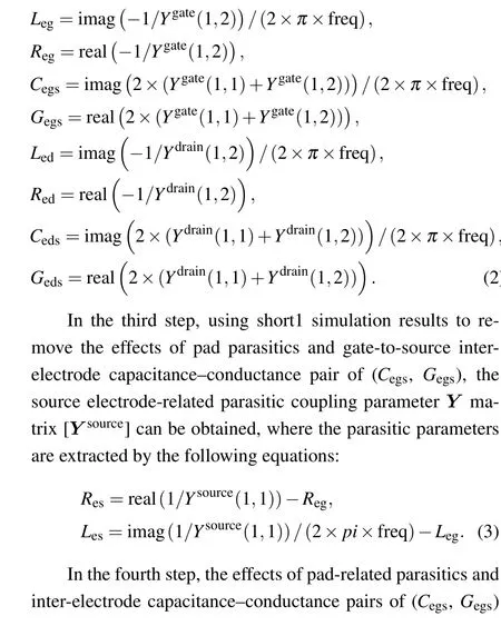
In the second step, by de-embedding the pad-related parasitics from the thru1 and thru2 test structure simulation results,the admittance matrix of the gate electrode-related parasitic couplings[Ygate]and the admittance matrix of the drain electrode-related parasitic couplings [Ydrain] can be obtained respectively. The parasitic parameters are extracted from the following equations:
Finally, in step five, the parasitic effects of parallelconnected pads and the parasitic effects of the device electrodes in series are excluded from the open simulation data,and the inter-electrode parasitic coupling parameterYmatrix[Yopen] is obtained, in which the inter-electrode capacitance and conductance parasitic parameters are given by the following equations:
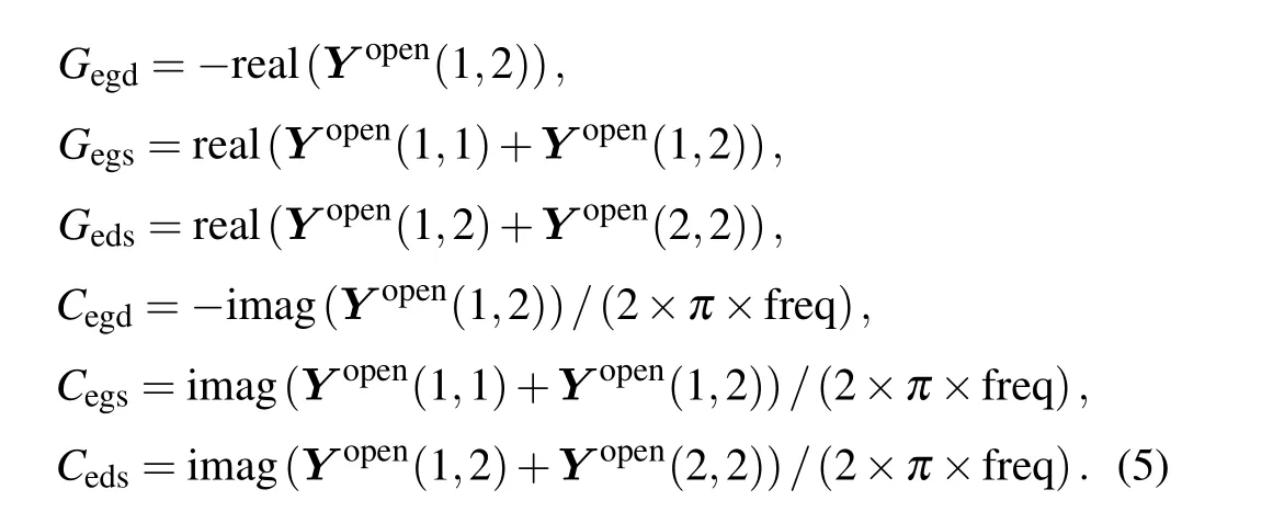

Fig.5. InP HEMTs extrinsic circuit model proposed for different representative test structures: (a)pad,(b)thru1,(c)thru2,(d)short1,(e)short2,and(f)open test.
4. Experimental verification of proposed equivalent circuit model
To validate the accuracy of the InP HEMT parasitic equivalent circuit above, here we use the HFSS simulations of the InP HEMT topology shown in Fig.2 in a frequency range of 1 GHz-40 GHz. All six proposed test standards are fabricated on a 3-inch InP wafer by depositing a single-layer of Au. The interconnect metallization is fabricated via Au evaporation,and the final Au layer has a thickness of 0.3µm. The parameter settings of the substrate and gold in the HFSS simulation are shown in Table 1, which are in accordance with the characteristics of the process materials used in our laboratory. TheS-parameters of the fabricated test patterns are measured by using the test platform in our laboratory in a range of 1 GHz-40 GHz band. The predicted and measuredS-parameters are compared with each other to highlight the degree of agreement between the frequency responses obtained from the HFSS simulations and the experimental data.
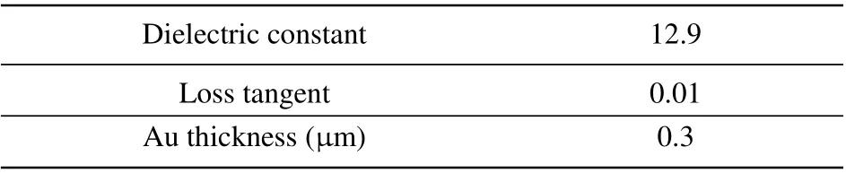
Table 1. Parameter settings of substrate and gold in HFSS simulation.
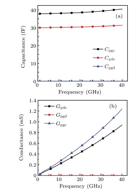
Fig.6. Capacitances and conductances associated with the device pads: (a)Cpgs,Cpds,and Cpgd;(b)Gpgs,Gpds,and Gpgd.
The gate, drain, and source inter-pad capacitances and conductances (Cpgs,Gpgs), (Cpgd,Gpgd), and (Cpds,Gpds) are shown in Figs. 6(a) and 6(b), respectively. In the pad structure, the gate and drain electrodes are removed, leaving only the corresponding two small pieces of metal pads and they are farther apart,so the extracted feedthrough capacitanceCpgdbetween the gate and the drain pad is at least 3 orders of magnitude smaller than the remaining capacitances as can be seen from the result graph. As such,Cpgdis often omitted in many similar external equivalent circuits reported in Ref.[18].In addition,the substrate conductance increases with the frequency increasing, and the substrate conductanceGpgdis different from the other two conductances by 3 orders of magnitude as can be seen from Fig.6(b).
The resistance and inductance of gate, drain, and source electrode are respectively(Reg,Leg),(Red,Led),and(Res,Les),and their results calculated in the second step are plotted in Figs. 7(a) and 7(b). Owing to the similar structures of thru1 and thru2, the resistancesRegandRedhave the same trend as shown in Fig. 7(a). The reason why the resistanceResincreases sharply with frequency increasing is the skin-effect of the current,which corresponds to the concentration of current flowing on the surface of the conductor at high frequency.[19]Figure 7(b) shows that the inductance of the gate, drain and source decrease as the frequency increases. The reason is that in the high-frequency skin-effect region, there is a vertical substrate current, which leads the line inductance to decrease.[20]As the operating frequency moves well into the mmW regime,the influence of mutual inductive gate-to-drain coupling becomes more pronounced,which necessitates its accurate characterization.[21]
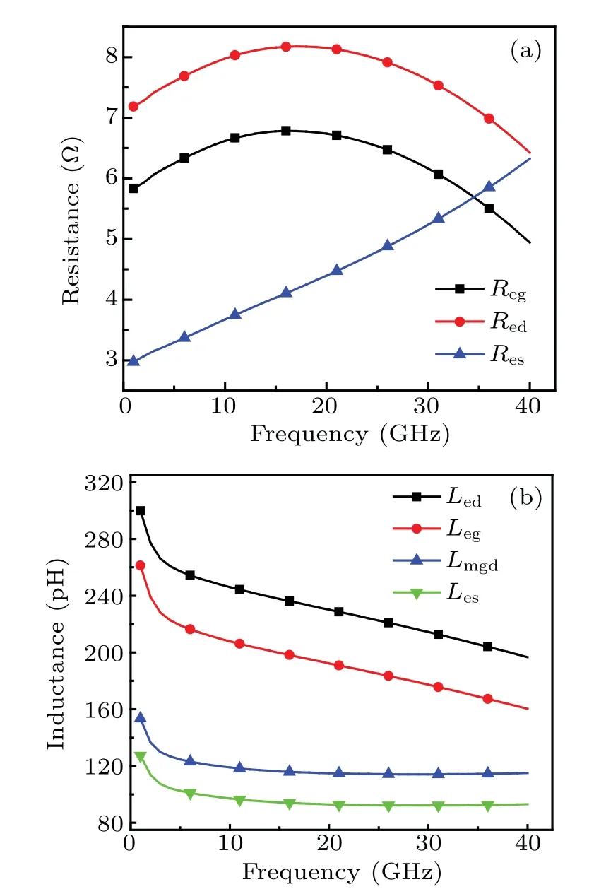
Fig. 7. Device electrode-related resistance and inductance terms. (a) Reg,Red,and Res;(b)Leg,Led,Les,and Lmgd.
The conventional InP HEMTs external parasitic equivalent circuit does not generally distinguish between the capacitance between pads and the capacitance between electrodes.[22,23]However, in order to maintain the modeling accuracy well in the mmW frequency range,the inter-pad coupling capacitance and the inter-electrode coupling capacitance need to be treated independently as done in this work. The calculated values of inter-electrode capacitance and conductance of(Cegs,Gegs),(Cegd,Gegd),and(Ceds,Geds)are given in Figs.8(a)and 8(b). Compared with the inter-pad capacitance and conductance proposed by the pad structure, the values of inter-electrode capacitance and conductance extracted by the open structure are slightly large because the metal of the open structure is intact and the electrode metal is not removed. In particular,the conductanceGegdbetween the gate and the drain varies significantly with frequency as can be seen in Fig.8(b).

Fig.8. Curves of frequency-dependent inter-electrode capacitance and conductance: (a)Cegs,Cegd,and Ceds;(b)Gegs,Gegd,and Geds.
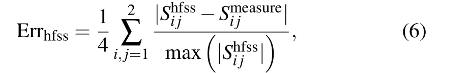
In order to verify the feasibility of the employed extraction of parasitic parameters and the accuracy of the InP HEMT equivalent circuit model, the HFSS simulation prediction, the measurement of the test structure and the modeledS-parameters are compared with each other as shown in Figs.9 and 10. Bring the pad parasitic parameters extracted in the first step of the pad simulation and the parasitic parameters of the device electrodes extracted in the second and third step into the corresponding equivalent circuit,theS-parameter comparison results are shown in Fig.9. TheS-parameters obtained from the HFSS simulation exhibit excellent agreement with the measured data on the 40-GHz bandwidth. Perhaps more importantly,the simulatedS-parameters of the proposed equivalent circuit given in Figs.5(a)-5(d)can very accurately reproduce the frequency response of the parasitic coupling in the band range of 1 GHz-40 GHz.
To further establish the validity of the extraction method and modeling, the complete set of parasitic coupling effects is estimated by executing the five steps of the proposed parasitic extraction algorithm. Following this, the extracted element values are substituted into the equivalent circuit of the short2 in Fig.5(e)and open test structure in Fig.5(f). As can be seen from Fig. 10, the simulated, measured, and modeledS-parameters for the two test standards of parameter extraction are shown again to be in excellent agreement with each other.
To evaluate the accuracy of the HFSS simulation method,the HFSS error is defined as follows:
where Errhfssis the error between the HFSS simulation value and the measure value,Shfssrepresents theS-parameter of the HFSS simulation,andSmeasuredenotes theS-parameter of the measurements. Through calculation, the error at 40 GHz is only 2.64%which is sufficiently small for most modeling application.
The good agreement between the HFSS simulation results and the test results shown in Figs. 9 and 10 demonstrates the accuracy of the HFSS EM simulations in predicting the measuredS-parameters on the 40-GHz bandwidth. The good agreement between the equivalent circuit simulation results and the test results proves the authenticity and accuracy of the equivalent circuit. More importantly, theS-parameters obtained from the equivalent circuit simulation can very accurately track the behavior of EM interaction. As seen in Figs.10(d)and 10(e),transmission coefficientS21of the open standard increases with frequency increasing, which shows that the insertion loss decreases with frequency increasing.The reason is that as the frequency increases,the capacitanceCegdbetween the gate electrode and the drain electrode plays a major role, providing an RF current flow path, so that the capacitive reactance continues to decrease.[24]This example clearly illustrates the dramatic frequency-dependence of parasitic couplings in the microwave-to-mmW regime.
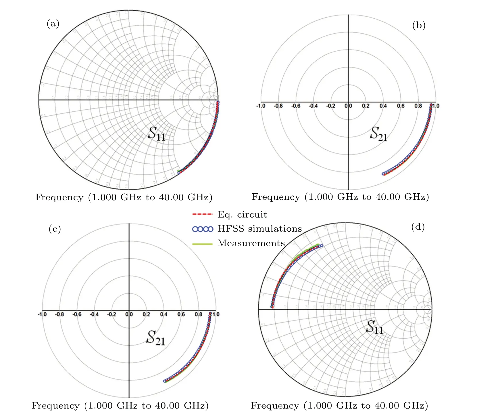
Fig.9. The S-parameters from HFSS simulation,measurement,and circuit model for pad,thru1,thru2,and short1 test standards: (a)S11 of pad,(b)S21 of thru 1,(c)S21 of thru 2,and(d)S11 of short1.

Fig.10. The S-parameters from HFSS simulation,measurement,and circuit model for short2 and open test standards: (a)S22 of short2,(b)S11 of open test,(c)S12 of open test,(d)S21 of open test,(e)logarithmic magnitude of S21 of open test,and(f)S22 of open test.
Figure 11 shows the comparison between simulation results without and with the gate-to-drain mutual inductanceLmgdin the InP HEMT parasitic equivalent circuit. The equivalent circuit withoutLmgdcannot accurately represent the frequency response of InP HEMT parasitic coupling in the band range of 10 GHz-40 GHz as can be seen from the figure.The transition from capacitive RF current transport at low frequency to inductive current transport at mmW frequencies is captured accurately with the aid of gate-to-drain mutual inductance ofLmgd. Hence, it is necessary to incorporate gateto-drain mutual magnetic flux linkage as a separate circuit element into the parasitic equivalent circuit of the InP HEMTs to maintain modeling accuracy at mmW band.
In order to further demonstrate the utility of the proposed methodology, a conventional cold-HEMT extraction method[16]is also employed to estimate the equivalent-circuit parameters based on the simulation data of the same InP HEMT layout. The extracted circuit element values are shown in Table 2.As can be seen,the conventional extraction method includes 9 equivalent circuit elements,and the element values,especially the resistances and inductances, deviate substantially from those calculated by using multi-step simulationbased procedure (see Figs. 6-8). It is also important to underline that achieving close agreement between the frequency responses of the equivalent circuit established by the conventional method and actual device may not necessarily mean that the calculated component values are physically representative.That is, the proposed extrinsic equivalent circuit in Fig. 5(f)contains 19 elements. Consequently,it is necessary to develop a multi-step device modeling strategy,thereby precisely determining the parasitic equivalent circuit of InP HEMT as presented here.
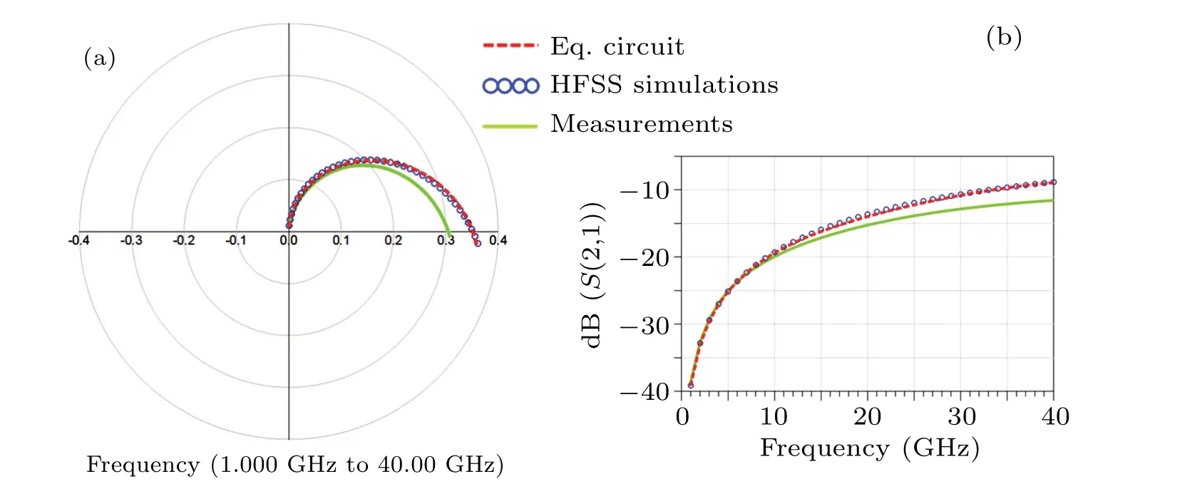
Fig.11. Comparison between simulated and modeled transmission coefficient S21 for open test structure with and without gate-to-drain mutual inductance component Lmgd,where Y Lmgd means that Lmgd is present,and N Lmgd means that Lmgd is absent,showing(a)polar S21 and(b)logarithmic S21.

Table 2. Element values extracted by conventional cold-HEMT extraction method.
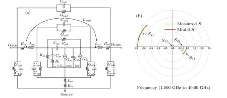
Fig.12. (a)Small signal equivalent circuit model of InP HEMTs and(b)fitting result of S-parameters.
The next step in HEMT characterization is to evaluate the influence of parasitic couplings on the high-frequency performance of InP HEMT. In order to do so, the intrinsic smallsignal equivalent-circuit parameters of a demonstrated device from our laboratory are combined with the extrinsic parasitic couplings extracted by using the full-wave simulation-based methodology described in this paper. The small signal equivalent circuit diagram of the complete InP HEMT can be obtained as shown in Fig. 12(a). After that, the topology is simulated and all values of parasitic parameters and intrinsic parameters are tuned to fit the model in the ADS. The fitting result ofSparameters for the model is demonstrated in Fig.12(b). As we can see,the curved portion in the low-and high-frequency range ofSparameters can be fitted by the small signal equivalent circuit model,showing good fitting.
5. Conclusions
We have demonstrated an extrinsic equivalent circuit model for the parasitic coupling of a two-finger InP HEMT.In addition, using the equivalent circuit extraction method of HFSS and ADS co-simulation,the InP HEMT topology is systematically partitioned,and allows for the straightforward determination of parasitic circuit elements. In the process of cosimulation extraction, the gate-drain mutual inductanceLmgdis introduced to improve the incomplete accuracy of the conventional model in high frequency modeling. The feasibility of the parameter extraction method and the accuracy of the model are demonstrated via comprehensive comparisons between simulated and measured equivalent-circuit frequency responses of the proposed test standards on a bandwith of up to 40 GHz. Subsequently, the small signal modeling and fitting results of InP HEMT prove the accuracy of the parasitic model. Finally, the practicality of the HFSS EM simulation tool serving as an alternative to fabrication and measurementbased equivalent-circuit extraction is verified to be a costeffective solution to optimizing the InP HEMT device performance.
Acknowledgements
Project supported by the National Natural Science Foundation of China(Grant Nos.61434006 and 61704189)and the Fund from the Youth Innovation Promotion Association of the Chinese Academy of Sciences.
猜你喜欢
科技进步与对策(2021年24期)2022-01-04
科技进步与对策(2021年22期)2021-11-26
科技进步与对策(2021年21期)2021-11-11
科技进步与对策(2021年16期)2021-08-25
科技进步与对策(2021年15期)2021-08-06
大众文艺(2021年3期)2021-03-15
科技进步与对策(2020年20期)2020-10-31
科技进步与对策(2020年19期)2020-10-15
科技进步与对策(2020年12期)2020-07-03
华中师范大学学报(人文社会科学版)(2020年3期)2020-06-17
- Chinese Physics B的其它文章
- Quantum walk search algorithm for multi-objective searching with iteration auto-controlling on hypercube
- Protecting geometric quantum discord via partially collapsing measurements of two qubits in multiple bosonic reservoirs
- Manipulating vortices in F =2 Bose-Einstein condensates through magnetic field and spin-orbit coupling
- Beating standard quantum limit via two-axis magnetic susceptibility measurement
- Neural-mechanism-driven image block encryption algorithm incorporating a hyperchaotic system and cloud model
- Anti-function solution of uniaxial anisotropic Stoner-Wohlfarth model