
Ceramic-copper substrate technology introduction
2022-07-26 08:18ZhaoQingqingSunWentao
China Welding 2022年2期
Zhao Qingqing , Sun Wentao
1. WLP&TPAK department, Shenzhen STS Microelectronics Co-Ltd, Shenzhen 518000, China;2. Quality department, Shenzhen STS Microelectronics Co-Ltd, Shenzhen 518000, China
Abstract Ceramic-copper substrate is used to achieve the combination between copper and ceramic (Al2O3 or AlN) under high temperatures by bonding or brazing process, then through dedicate lamination – etching technology to develop the designed layout in copper surface,finally parts go with plating and singulation process for surface treatment before shipping to the end-user. Ceramic-copper substrate has perfect performance in terms of insulation, thermal conductivity, solderability, and adhesion strength. Besides, the copper on surface can afford huge current due to the fact that ceramic has good reliability and thermal-cycling performance. According to technical visit and audit to suppliers’ manufacturing process and based on several years’ experience of mass production for electric vehicle power module package, this article introduces two mainstream ceramic-copper substrate processing methods currently on the market: direct bond copper (DBC) and active metal brazing (AMB) which can be widely used for the intelligent power module and electric vehicle power module, also introduces the major failure mode during application and analyzes the root cause for each failure mode, clarifies key incoming monitoring method, like crosshatch, silver plating thickness measurement and blister test. This article also clarifies the Incoming Quality Control system, which can provide guidance to process engineer during the application.
Key words copper, ceramic, bonding/brazing, power module
0 Introduction
In recent years, with the rapid development of power semiconductor, and with the characteristics of wide band gap and high thermal conductivity of the third-generation semiconductor silicon carbide chip, the ceramic-copper substrate, as a chip carrier, has been applied to carry the chip and connect to the water-cooling system (welding or sintering) in the application of end customer, so as to achieve the high heat dissipation, reliability and insulation performance required by the chip[1]. At present, the new power semiconductor module based on ceramic-copper substrate has been put into mass production in major semiconductor companies, such as ST Semiconductor, Infineon and ON Semiconductor. The demand for and the quality requirements on ceramic-copper substrate in the industry are increasing, and so it is urgent for the engineers in the semiconductor industry to get aware of the manufacturing process and application risks of ceramic-copper substrate. According to the on-the-spot audit of major manufacturers of ceramic-copper substrate (Rogers/Denka/Heraeus/Ferrotec), including benchmarking of procedures, equipment and quality control,and based on the nearly three years’ manufacturing experience, this article introduces two mainstream ceramic-copper substrate processing methods on the market: direct bond copper (DBC) and active metal brazing (AMB), and clarifies the application risks, incoming monitoring methods and indicators.
1 Introduction to DBC and AMB
1.1 Direct bond copper
DBC is a composite substrate made by bonding the copper directly to the surface of Al2O3or AlN ceramic at high temperatures and through hot-melt bonding method. On the copper-clad surface, the corresponding pattern can be etched based on circuit design or product structure. It has been widely used for the package of intelligent power module and electric vehicle power module[2].
1.2 Active metal brazing
AMB technology, a further development of DBC technology, is a method to achieve the combination of ceramic and metal by utilizing the active metallic element in the solder (such as Ti/Ag/Zr/Cu). The ceramic forms a reactive layer that can be wetted by liquid solder.
The combination in AMB substrate is achieved through the chemical reaction of ceramic and active metal brazing solder at thigh temperatures. Compared with traditional Al2O3ceramic substrate, the Si3N4ceramic used in AMB has higher thermal conductivity (> 90 W/mK@25 °C),which is closer to the thermal expansion coefficient of silicon (2.6 ×10⁻⁶/K). Therefore, AMB substrate is of higher adhesion strength and reliability. In combination with silver sintering process and high-power silicon carbide chip, the AMB copper layer with active metal coating could realize a package module with high power, better heat dissipation and high reliability (withstand thermal shock of 3 000 cycles)[3], which has been widely applied in electric vehicles, power locomotives and high-speed train. The performance comparison between DBC and AMB is shown in Table 1.
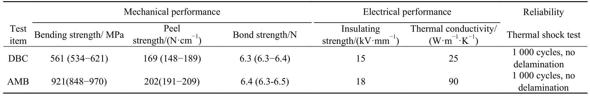
Table 1 Performance comparison between DBC and AMB
2 Technical process
The overall technical process of ceramic-copper substrate is as follows: firstly, carrying out surface treatment on supplied copper and ceramic; then, stacking the copper and ceramic and placing them into vacuum high-temperature furnace for soldering; after that, carrying out chemical etching of copper on surface of ceramic to generate designed pattern and lines; and then, cutting the ceramic substrate with laser, and carrying out singulation to obtain single chip[4].
There are two main differences between DBC and AMB product: firstly, the copper and ceramic of DBC product are bonded directly, while the copper and ceramic of AMB product are brazed by using active metal brazing solder, for which the additional screen printing process shall be carried out before brazing to place active metal brazing solder on ceramic substrate evenly; secondly, the copper of DBC product is formed through one time of etching, while for AMB product with an additional metal brazing solder layer,an additional etching process shall be carried out to remove the brazing solder, for which the hydrofluoric acid is usually adopted.
Taking AMB product as an example, the technical process of ceramic-copper substrate is shown in Fig. 1, and the main processes and materials will be introduced in detail below.
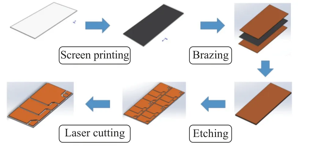
Fig.1 Processing technology of AMB ceramic-copper substrate
2.1 Raw materials
The direct raw materials of ceramic-copper substrate mainly include copper strip and ceramic substrate, as well as special active metal brazing solder (in case of AMB).
Copper strip: at present, the Cu-OFE (with copper>99.99%, oxygen <0.000 5%) is widely used in the industry. It is supplied in the form of strip and shall be pressed and cut to form the copper foil with the same size as supplied ceramic before usage. Since the chemical pretreatment shall be carried out before bonding, the storage life of copper strip is not required strictly.
Active metal brazing solder: It is a mixed paste material with certain adhesiveness. In order to prevent any change in its characteristics, it is usually stored at subzero temperature, and shall be thawed and mixed immediately before usage. The current common suppliers include Tong Hsing,Ecocera, ICP etc.
Ceramic: The ceramic materials used in AMB and DBC are different. The ceramic materials used in DBC mainly include Al2O3and AlN, where Al2O3is more mature than AlN in technology and has advantages in price, and so has been adopted used in 80% of the DBCs on the market. The ceramic material used in AMB is Si3N4with higher thermal conductivity. Si3N4is supplied in the form of powder, and can be processed into the ceramic wafer required by AMB production after a series of mixing, blending, printing and forming. In recent years, the demand for Si3N4powder of the major ceramic-copper substrate manufacturers has increased significantly, but most of the suppliers of Si3N4powder in the industry are in Japan, such as Denka,Maruwa, Toshiba and Tokutama. Powder type is as shown in Fig. 2, flaky type is as shown in Fig. 3, and the manufacturing technology of ceramic wafer is as shown in Fig. 4.

Fig.2 Si3N4 powder
Fig.3 Flaky Si3N4

Fig.4 Manufacturing technology of Si3N4 ceramic wafer
2.2 Screen printing
Immediately before the screen printing, the active metal brazing solder shall be taken out from the environment with subzero temperature and placed at the room temperature for a while to ensure the adhesiveness and printing properties.Before printing, the thawed active metal brazing solder shall be centrifugally stirred to remove the bubbles in the solder and ensure the sufficient mixture of solvent and active agent, thus preventing the lack of solder during printing.The detailed printing process is as shown in Fig. 5.
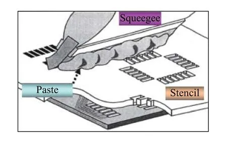
Fig.5 Introduction to screen printing process
In order to ensure that sufficient solder is left on surface of ceramic wafer after printing, the ceramic wafer shall be weighed before and after printing for comparison. In case of any abnormality in thickness of printing, the solder printed on the surface can be cleaned by using alcohol pad and carry out printing again.
Screen printing is a mature process for the placement of soldering/brazing material and has been processed in few abroad suppliers such as Rogers and Denka. However, instead of screen printing, preform is also used in domestic production plant of some supplier such as Ferrotec. Comparing to screen printing, preforms can be easily transported and stored, which is believed to lower the cost. Besides,the using of preforms will significantly improve the bonding quality by eliminating the voids in the bonding/brazing process.
2.3 Bonding/ brazing
To combine copper and metal in DBC preparation, the oxygen element will be introduced between the copper and ceramic substrate; then the eutectic phase will be formed at 1 065 °C; after that, the ceramic substrate will react with copper to generate CuAlO2or Cu(AlO2)2, thus to realize the eutectic bonding between copper and ceramic. The process principle is as shown in Fig. 6[5].
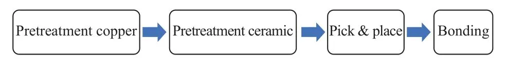
Fig.6 Introduction to bonding process
After surface treatment, copper and ceramic will be picked and placed in the loading place of vacuum furnace,and then be placed into the furnace chamber for bonding.The bonding process is the core of whole DBC technical process, and is the bottleneck affecting the yield (some domestic suppliers can only realize the yield of 90%). The defects affecting yield is the bubble between copper and ceramic.
In AMB preparation, the active metal solder is utilized to combine copper and ceramic substrate. The brazing solder containing Ti/Ag/Cu[6– 7] and other elements can have chemical reaction with ceramic to generate the reaction layer that can be wetted by liquid solder[8–9], thus to realize soldering of metal on surface of ceramic without metallization. The process principle is as shown in Fig. 7.

Fig.7 Introduction to brazing process
According to the cross-section shown in the following Fig. 8, the brazing solder is located between copper and ceramic, whose main element is Ag-Cu.

Fig.8 Picture of AMB cross-section
AMB substrate preparation technology is the development of DBC technology. The active metal brazing solder is adopted to bring down the bonding temperature, thus to reduce the thermal stress in the ceramic substrate. Since the bonding of AMB substrate is realized by utilizing the chemical bond generated in chemical reaction between active metal solder and ceramic, and the Si3N4used in AMB is of higher thermal conductivity than Al2O3used in DBC, the AMB substrate can achieve better heat dissipation and insulation performance and higher reliability, and therefore it could be used to carry chips with larger power which are mostly used in electric vehicle power module. The DBC substrate is usually adopted in refrigerator, air conditioner and other consumer electronics with medium and small power.
At present, the preparation of active solder is the key technology for preparation of AMB substrate. The active metal solder can be classified as high-temperature solder(active metal includes Ti, V and Mo, of which the soldering temperature is 1 000−1 250 °C), medium-temperature solder(active metal includes Ag-Cu-Ti, carrying out soldering in protective gas or vacuum at 700−800 °C,) and low-temperature solder (active metal includes Ce, Ga and Re at the soldering temperatures of 200−300 °C)[10]. With simple composition, easy operation and high mechanical strength, the high and medium-temperature active solder has been widely applied in metal-ceramic combination.
The bubble is also a key defect for AMB brazing process. Therefore, the ultrasonic scanning is introduced after the bonding/ brazing process to detect the bubble under copper generated in bonding/ brazing process. Since the hidden bubble will affect the overall heat dissipation of semiconductor module and so result in reliability risk when defective product is delivered to the semiconductor factory, the semiconductor factory will carry out reliability test during verification of ceramic-copper substrate, including SAM(ultrasonic scanning) test after 3 000 cycles of thermal shock, thus to check whether there is any delamination between copper and ceramic.
2.4 Lamination-etching
The etching pattern of ceramic-copper substrate is formed through the lamination- etching process, as shown in Fig. 9.
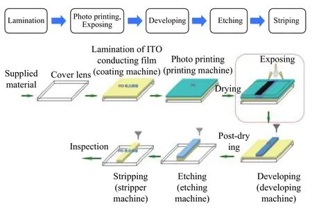
Fig.9 Lamination-etching process
Lamination: A layer of ITO conducting film (Indium Tin Oxide) will be plated onto the overall master card for electric conduction, as shown in Fig. 10.
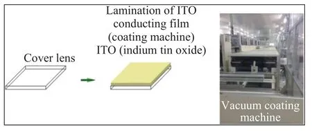
Fig.10 Lamination
Photo printing:Plated photoresist material on surface of master card with ITO and baked it. Yellow light is necessary during process due to high sensitivity of photoresist material, as shown in Fig. 11.
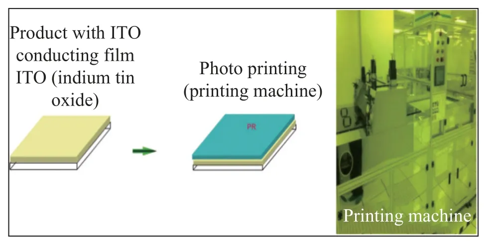
Fig.11 Photo printing
Exposing: The ultraviolet light will penetrate through the mask and hit the photoresist surface of product to be exposed. The ultraviolet light can penetrate the transparent part of the mask and hit the photoresist to cause reaction of the photoresist, but it cannot penetrate through the nontransparent black part of the mask to cause reaction. By this way, the pattern on the mask can be projected to the photoresist coating on the master card, as shown in Fig. 12.

Fig.12 Exposing
Developing: After exposing, the developing solution will be sprayed on the product surface to dissolve and remove the photoresist that has had reaction from the surface of master card. The part that is not exposed to ultraviolet light and does not have reaction will be kept on surface of master card, as shown in Fig. 13.

Fig.13 Developing
Etching: After being processed with developing solution, the master card with pattern will be dipped into the acid solution for corrosion. The part of copper on surface of master card that is not covered with photoresist will be etched off, leaving the part being protected by photoresist to form etching pattern, as shown in Fig. 14. The brazing solder under copper will not be etched by acid solution. The etching depth can be controlled by controlling the concentration of acid solution and immersing time of master card(speed of steel belt) in manufacturing procedure.
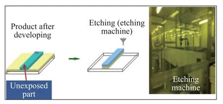
Fig.14 Etching
Striping: as shown in Fig. 15, the stripping liquid will be sprayed on the surface of master card after etching. The stripping liquid will dissolve the remained photoresist on the surface of master card to expose the surface of copper that is not etched, and by this way the etching pattern of first layer is formed.

Fig.15 Striping
As for the lamination- etching process, the etching depth is an important IPC monitoring item. This is usually measured and the CPK performance will be monitored after stripping.
2.5 2nd lamination -etching
As for DBC product, the final pattern can be formed by one time of etching. But in preparation of AMB substrate,the lamination-etching process shall be repeated as there is an extra layer of brazing solder, but the type of etching solution shall be adjusted accordingly, for example, the hydrofluoric acid can be used to remove the brazing solder to show the ceramic substrate, thus to let the lines on surface of AMB meet requirements on electric performance.
2.6 Plating
According to the subsequent application in client side,the surface of ceramic-copper substrate can be provided with different coatings, and the coatings commonly adopted in the industry include silver, gold, and nickel coating etc. The silver-plating process will be taken as the example for elaboration, as shown in Fig. 16.

Fig.16 Silver plating process
In prior to chemical plating, the copper on surface of ceramic-copper substrate shall be cleaned to remove the foreign bodies. The substrate with clean surface shall be subjected to acid treatment again to remove the oxides on surface. After that, the substrate shall be etched and be dipped into the plating bath to complete surface plating, and finally,the surface of substrate shall be cleaned and dried.
The plating thickness is an important IPC monitoring item for plating process. The XRF (X-ray fluorescent spectrometry) can be adopted to measure plating thickness and carry out CPK monitoring. According to the current monitoring, the plating thickness in different places of an overall master card may vary considerably, which may result in large fluctuation of plating thickness in whole batch, affecting the application of customers.
2.7 Laser cutting
After the chemical plating, the pre-cutting of master card will be carried out with industrial laser and along the sawing street, thus to prepare for the subsequence manual singulation. Since the copper has undergone etching, the laser cutting mainly acts on the sawing street between singe chips on the ceramic substrate, for which the cutting depth shall be controlled strictly. The mainstream laser in the industry includes CO2laser (carbon dioxide laser, as shown in Fig. 17) and USP laser (ultrashort pulsed laser)[11].
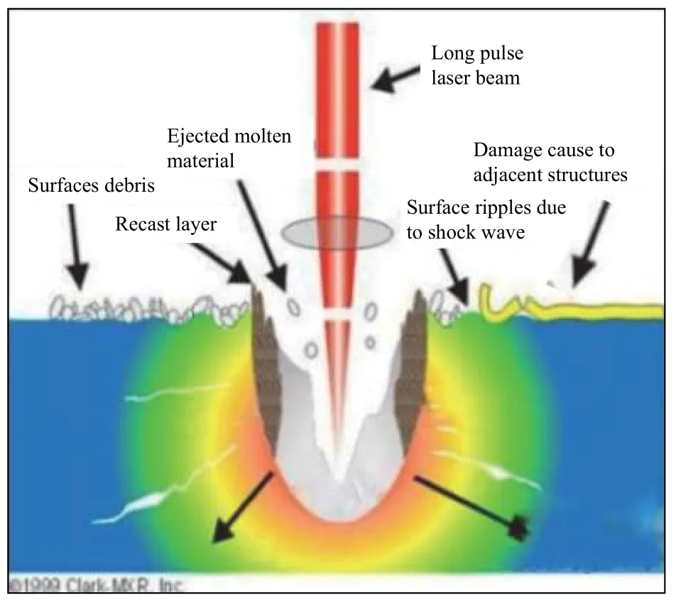
Fig.17 Schema of CO2 laser cutting and damage casued
CO2laser is a gas molecule laser, where the working substance is CO2, the auxiliary gas includes nitrogen, helium, hydrogen and xenon. Utilizing the vibration of CO2molecule and transition between rotational energy levels to generate the infrared laser with wavelength of 10.6 μm, the CO2laser is of higher energy conversion efficiency, larger power, higher optical quality of laser beam, better coherence and higher working stability, and so it is usually used for industrial metal cutting.
The cutting mode of CO2laser is single-point impact,which can cause deep damage to ceramic substrate, as shown in Fig. 18[12].
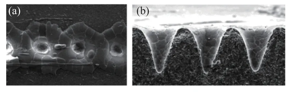
Fig.18 SEM picture of (a) surface appearance and (b) surface section under single-point impact
The so-called ultrashort pulse used in USP laser (ultrashort pulsed laser) is femtosecond laser pulse. Fig. 19 shows the generation principle of typical titanium doped sapphire crystal laser[13]:

Fig.19 Diagram of oscillation structure of femtosecond laser
With the wavelength of nanoscale and the peak power of petawatt (1,015 watts), the ultrashort pulsed laser can realize concentration of energy in limited area for rapid processing. USP laser as shown in Fig. 20.

Fig.20 USP Laser
Compared with CO2laser, the USP laser can cause less damage to the sawing street on the ceramic and realize better cut surface forming[14]. Due to its obverse advantage,USP laser cutting is now taking place of CO2laser in some domestic plant and may be extended to oversea suppliers.Fig. 21 is the comparison of different laser.
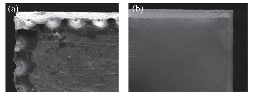
Fig.21 Comparison of scribed line (a) CO2 laser (b) USP laser
2.8 Singulation
Since the master card is not completely disconnected to form single ceramic-copper substrate after laser cutting, the singulation shall be carried out. The strength shall be controlled properly during singulation, thus to prevent edge chipping or cracking of ceramic wafer. After the singulation, the appearance full inspection on single chip shall be carried out, and corresponding defect shall be picked and recorded. The current common defects include scratch,broken corner, corrosion hole, leakage of copper and oxidic dirt etc.
3 Analysis of failure modes
3.1 Copper bridge (incomplete corrosion)
Copper bridge is the defect of ceramic-copper substrate that is common in etching process, which refers to failure in etching of required pattern due to incomplete exposure in the lamination- etching process, or incomplete removal in the developing process. Such defect will result in short-circuit of power module.
Fig. 22 shows the typical copper bridge on DBC substrate of power module, which can result in short-circuit of adjacent pins.
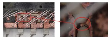
Fig.22 Copper bridge
3.2 Copper exposure
The biggest risk in practical production is copper exposure, which is caused by weak adhesion strength between coating and copper. The root cause of copper exposure is larger surface roughness of copper, and abnormal temperature or time of plating. Such defect will result in abnormity in push-pull force after sintering of chip and failure in module sintering by end customer.
Fig. 23 shows the typical copper exposure on back of AMB substrate of intelligent power module for electric vehicle.
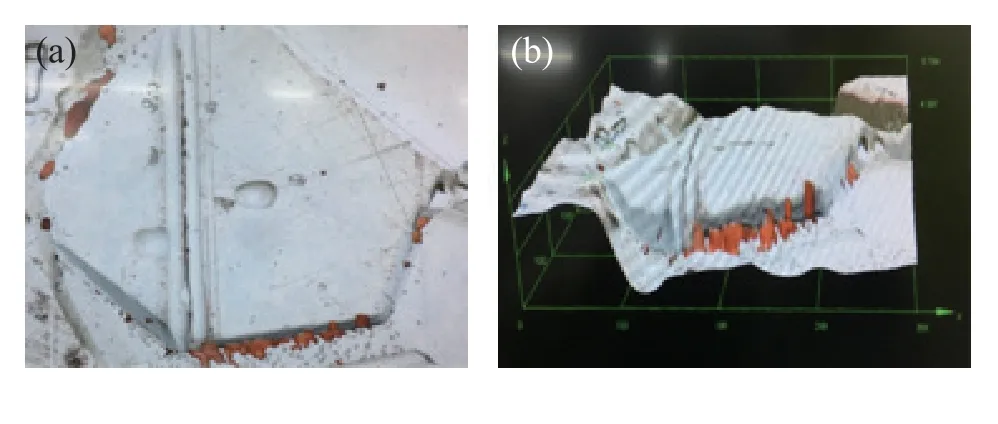
Fig.23 Copper exposure (a) under optical microscope and(b) under morphology scanner
3.3 Solderability issue
Solderability issue refers to poor solderability of ceramic-copper substrate surface, of which the common manifestation is non-stick of solder paste or tin flake on AMB/DBC surface after soldering in reflow furnace. This application risk cannot be detected through appearance inspection of supplied substrate and can only be found through solder wetting test. There are two root causes for this: firstly, the pretreatment of plating process is incomplete, resulting in bubble in copper surface and poor bonding of silver layer;secondly, residue generated during laser cutting is left on AMB surface, resulting in abnormality in surface clearance.Fig. 24 is an example of solderability issue
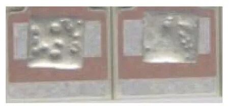
Fig.24 An example of solderability issue
3.4 Laser hole
Laser hole is the defect of ceramic-copper substrate occurred in CO2laser cutting process. The ceramic-copper substrate for mass production is usually designed with cutway to prevent placement in wrong direction. As shown in Fig. 25, the sawing street for singulation coincide with that for cut-way, and so repeated laser cutting will occur in specific area[15].
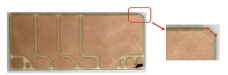
Fig.25 Laser hole
As shown in Fig. 26, since the cutting mode of CO2laser is single-point impact, the risk of penetration of ceramic substrate may be incurred when the center of the two laser points coincides during cutting of cut-way, which can result in stress concentration during subsequent loading and application of power module, leading to chipping of ceramic wafer, as shown in Fig. 26.
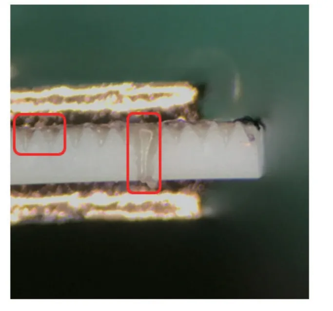
Fig.26 Chipping of ceramic wafer
4 Key incoming monitoring methods
4.1 Crosshatch
A common problem in substrate application is poor adhesion strength of surface coating, which will incur falling off of silver layer under impact of high-pressure water in subsequent application, and will seriously affect the corresponding sintering quality, affecting the application by end customer. Therefore, the crosshatch sample test on incomings can be carried out to monitor the adhesion strength of coating.
According to the regulations of ASTM D3359, the adhesion test will be carried out with 3M tape after cutting the substrate with cutting tool. The level of adhesion strength shall be judged according to the area of remained silver coating on surface, as shown in Table 2. According to the levels of grid test results, it has been found after formulating and completing a series of subsequent evaluations that the process requirements of semiconductor packaging industry can be met only when the test level is larger or equal to 4B.
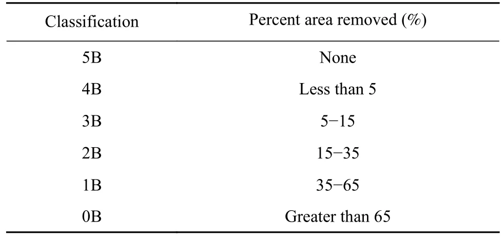
Table 2 Performance comparison between DBC and AMB rating scale for adhesion test
4.2 Ag thickness measurement
As for the ceramic-copper substrate with silver coating,the Ag thickness has significant influence on stability of surface sintering process. Therefore, Ag thickness is an important indicator for IQC monitoring, and it is usually 0.1−1.0 μm. For the ceramic-copper substrate with other coatings (nickel/ tin coating etc.), the thickness can reach 10 um. This plating process is relative stable, and the control of plating thickness is relatively accurate, and therefore the control of plating thickness is not required.
The equipment used for measurement is XRF-FT150 high-precision plating thickness tester, and the measuring time of each single-point Ag thickness is 100s. In measurement with XRF equipment, the standard chip shall be adopted for calibration, with each kind of standard chip covering the measurement range of 1/2 −2 times of standard chip thickness. Meanwhile, great measurement system fluctuation shall be guaranteed before measurement (gage R&R<10%).
4.3 Blister test
Blister test is also known as “bubble test”. According to the regulations in ASTM B571, the substrate shall be dipped into the deionized water at 220 °C for 1 hour, and then be placed into the water of 25 °C±5 °C to cool it to room temperature; and finally, the microscope will be used to observe whether there is any bubble on the coating. The cracking or peeling of coating suggests abnormal adhesion strength of coating.
5 Conclusions
(1) Based on the mass production experience and technical accumulation of recent years, this article introduces the process, application risks, incoming monitoring methods and others for the current mainstream ceramic-copper substrate.
(2) With the development of electric vehicle industry and continuous development of silicon carbide chip technology, the large power semiconductor module using ceramiccopper substrate will become the mainstream in the following years. High reliability, low void rate and low cost,which are related with ceramic-copper materials and technical path chosen, are aims that both domestic and overseas suppliers make effort to achieve.
(3) Based on above introductions, the semiconductor engineer could establish the incoming monitoring system according to the typical defects and application risks of ceramic-copper substrate in advance, trace each production process of material supplier quickly in case of quality accident,and analyze the issue of poor connection of substrate and cooling system of final client. In the power module application field, the ceramic material and heat dissipation package mode changes with each passing day. It is hoped that this paper could help the engineers to have in-depth understanding of this field, and help to apply relevant knowledge to solve corresponding problems in the future work and technical researches.
- China Welding的其它文章
- The study of arc behavior with different content of copper vapor in GTAW
- Research on stretching flame correction technology of aluminum alloy ship frame skin welding structure
- Application of silver nanoparticles in electrically conductive adhesives with silver micro flakes
- Groove modeling and digital simulation for intersecting structures of circular tubes based on coplanarity of vectors
- A novel single wire indirect arc metal inert gas welding process operated in streaming mode
- A review of welding residual stress test methods